
Circuit Diagram
Index 1318
CARRIER_CURRENT_REMOTE_CONTROL_OR_INTERCOM
Published:2009/6/24 23:34:00 Author:May
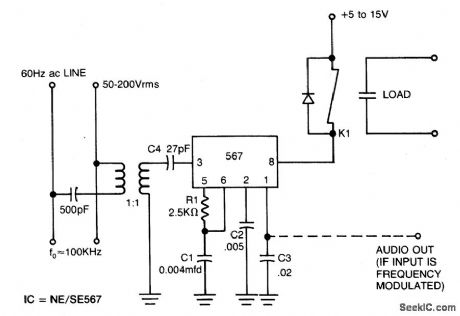
View full Circuit Diagram | Comments | Reading(674)
IMPEDANCE_CONVERTER
Published:2009/6/24 23:42:00 Author:Jessie
Used to match 10-megohrninputimpedanceto 50-ohm transmission Iine or 50-ohm input of instruments such as spectrum analyzer, video amplifier, or fre-quency counter. Voltage gain is exactly 0.5. Fre-quency response is from DC to 20 MHz and can be boosted by using higher-frequency transis-tor.-M. J. Salvati, FET Probe Drives 50-Ohm Load, EDN Magazine, March 5, 1973, p 87 and 89. (View)
View full Circuit Diagram | Comments | Reading(3038)
13_W_at_16O_MHz
Published:2009/6/24 23:32:00 Author:May
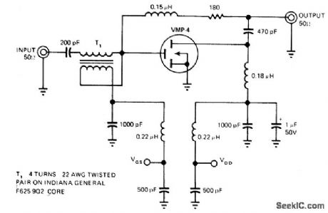
Circuit uses Siliconix VMP-4power MOSFET to provide 11-dB gain with 26-V supply、or 14 dB with 36-V supply,Broadband design permits operation over wide range of frequencies up to as high as 600 MHz.-RF Power MOSFET Outputs 13 W at 160 MHz wih High Gain、No Breakdown、EDNMagazine.June 20,1976、p 144-145 (View)
View full Circuit Diagram | Comments | Reading(699)
PHOTOCELL_MEMORY_SWITCH_FOR_AC_POWER_CONTROL
Published:2009/6/24 23:42:00 Author:Jessie
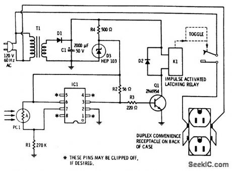
Provides remote control for ac-powered devices by using the beam of a flashlight as a magic wand. The important aspect of this gadget is that it remembers. Activate it once to apply power to a device and it stays on. Activate it a second time and power goes off and stays off. It consists of a combination of a high-sensitivity photocell, a highgain IC Schmitt trigger, and an impulse-actuated latching relay. (View)
View full Circuit Diagram | Comments | Reading(1497)
LOW_FREQUENCY_CRYSTAL_OSCILLATOR
Published:2009/6/24 23:31:00 Author:May
Circuit NotesThis crystal-oscillator circuit uses crystal. (View)
View full Circuit Diagram | Comments | Reading(0)
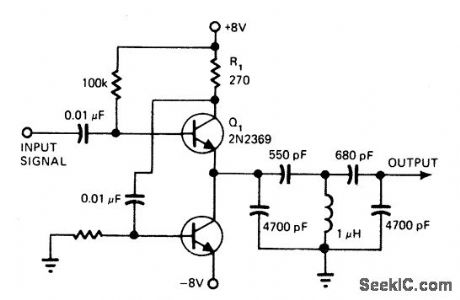
MULTIPURPOSE_MODULE
Published:2009/6/24 23:41:00 Author:Jessie
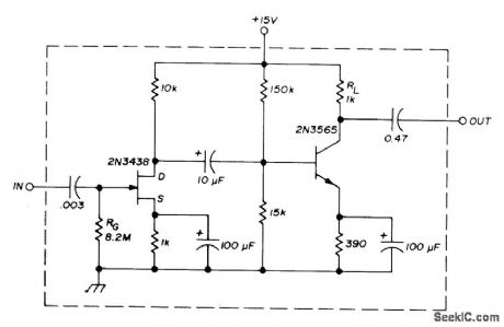
Flexible circuit using FET to drive bipolar transistor has -3 dB points at 100 Hz and 0.6 MHz. Components are noncritical and can be changed considerably in value to optimize gain, frequency response, power output, or power consumption. Load presented to FET is primarily input resistance of bipolar transistor, about 1000 ohms, which gives voltage gain of 4 for FET.-I. M Gottlieb, A New Look at Solid-State Amplifiers, Ham Radio, Feb. 1976, p 16-19. (View)
View full Circuit Diagram | Comments | Reading(1433)
SUMMING_SCALING_VIDEO
Published:2009/6/24 23:31:00 Author:May
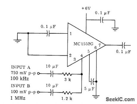
With Motorola MC1552G video amplifier connected as shown, summation of input signal currents is accom-plished at pin 4 through input resistors whose values arechosen to give desired scale factor.- A Wide Band Monolithic Video Amplifier, Mo-torola, Phoenix, AZ, 1973, AN-404, p 9. (View)
View full Circuit Diagram | Comments | Reading(663)
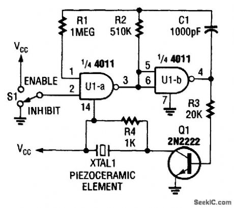
CMOS_PIEZO_DRIVER_USING_4049
Published:2009/6/24 23:41:00 Author:Jessie

This circuit uses a 4049 IC to drive a 2N2222 switching transistor The transistor drives crysbal 1 a ptezo transducer. (View)
View full Circuit Diagram | Comments | Reading(0)
2304_MHz_PREAMP
Published:2009/6/24 23:40:00 Author:Jessie
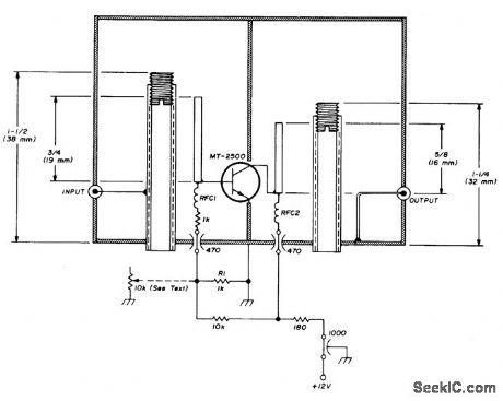
Narrow-band stage using Fairchlld MT-2500 bipolar transistor gives gain of 6 to 9 dB and noise figure of 2.5 to 4.5 dB.Cavity resonators at both input and output give excellent frequency selectivity. Similar circuit can be used wi1h Fairchild MT-4500, FMT-4005, or equivalent newer stripline-type transistors.RFC1 is 3 turns and RFC2 is 5 turns, air-wound with No. 26 enamel by using No. 52 drill as mandrel. Coupling strips on base and collector of transistor are 0.25-mm brass shim stock. Article gives construction and tune-up details, along with altemate design for HP-35821E and HP-35862E transistors using coupling loops. 10K pot is used only during tune-up.-N. J. Foot, Nanow-Band Solid-State 2304-MHz Preampli-fiers, Ham Radio, July 1974, p 6-11.
(View)
View full Circuit Diagram | Comments | Reading(776)
IC_CARRIER_CURRENT_RECEIVER
Published:2009/6/24 23:31:00 Author:May
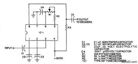
View full Circuit Diagram | Comments | Reading(971)
SMALL_SIGNAL_AMPLlFlER
Published:2009/6/24 23:31:00 Author:May
Combines fea-tures of virtual-earth and high-inpufimpedan ce amplifiers economically for such applications as a record amplifier, and provides several times the gain of a virtual-earth amplifier alone.-D.Rawson-Harris, Small Signal Amplifier, Wire-less World, Feb. 1977, p 45. (View)
View full Circuit Diagram | Comments | Reading(764)
CRYSTAL_OSCILLATOR_DOUBLER
Published:2009/6/24 23:30:00 Author:May
Circuit Notes
The crystal operates into a complex load at series resonance. L1, C1, and C2 balance the crystal at zero reactance. Capacitor C1 fine-tunes the center frequency. Tank circuit L2, C3 doubles the output frequency the circuit operates as an FM oscillator-doubler. (View)
View full Circuit Diagram | Comments | Reading(982)
CMOS_PIEZO_DRIVER
Published:2009/6/24 23:39:00 Author:Jessie
A CMOS-gate and transistor buffer can be used as an effective driver for a piezoelectric transducer. (View)
View full Circuit Diagram | Comments | Reading(0)
BASIC_FEEDBACK_AMPLlFlER
Published:2009/6/24 23:30:00 Author:May
Combination of unipolar and bipolar transistors gives desirable amplifying features of each solid.state device.Circuit can be optimized for RF or AF by ad justing coupling, feedback, and emitter bypass capacitor values. Changes in feedback affect dis-tortion, frequency response, and gain stability.To optimize for RF reduce capadtor sizes. For both AF and RF response, capacitors shown can be paralleled by small ceramic or Mylar units. If FET and bipolar are selected for high transcon-ductance and high gain-bandwidth product, overall voltage gain can be 20 or more for fre-quencies up to several megahertz.-I. M. Gott-Iieb,A New Look at Solid- State Amplifiers, Ham Radio, Feb. 1976, p 16-19. (View)
View full Circuit Diagram | Comments | Reading(932)
ENLARGER_EXPOSURE_METER
Published:2009/6/24 23:36:00 Author:Jessie
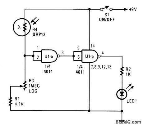
Two gates of a 4011 are used as a comparator. When the resistance of R4 decreases the voltage at pin 1 and 2 increases, producing a logic zero at pin 3, causing pin 4 to go high and activating the LED. R3 is calibrated in light units, or seconds exposure time. To calibrate, set pot R3 so as to just be on the LED ON/OFF threshold. With a light level that is suitable to correctly expose a photographic print, use a known enlarger and a known negative. (View)
View full Circuit Diagram | Comments | Reading(1377)
SINGLE_TRANSISTOR_CARRIER_CURRENT_RECEIVERTO_LINE_COUPLER
Published:2009/6/24 23:30:00 Author:May
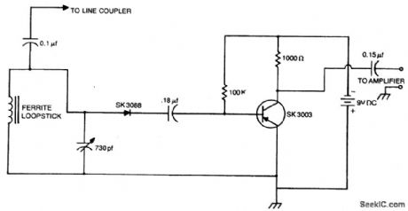
View full Circuit Diagram | Comments | Reading(653)
AC_WITH_IMMUNITY_TO_LARGE_DC_OFFSET
Published:2009/6/24 23:29:00 Author:May
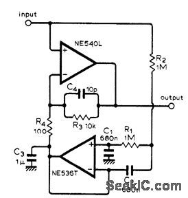
Designed to amplify from about 250 kHz down to Iow frequencies in presence of Iarge DC input offsets. Main NE540L ampllfier has gain of 101, while NE536T has DC gain of unity and forms part of Iow-pass network that applies DC input offset as common-mode voltage to inverting input of main amplifier.-A. Royston, Low Fre-quency A.C. Amplifier, Wireless World, May 1976, p 80. (View)
View full Circuit Diagram | Comments | Reading(743)
CAPACITIVE_LOAD_EMITTER_FOLLOWER
Published:2009/6/24 23:29:00 Author:May
Overcomes problem that develops with trailing edges of pulses when emitter-follower using NPN transistor is driving heavily capacitive load. Extra transistor is used to dump capacitor charge when emitter-follower stops conducting at trailing edge of input waveform. Pulse trailing edge thus tends to cut off a, and saturate lower transistor so it discharges capacitor. Circuit works equally well with pulses, square waves,and sine waves Transistors need not bematched Reverse polarity of supplies to usePNP transistors Useful for driving long coaxlines or logic from high-impedance source,without inversion,-H.L.Morgan,Emitter Follower's Fall Time Is Independent of Load、EDN Magazine Feb,5,1977,p 105 (View)
View full Circuit Diagram | Comments | Reading(1532)
IC_CARRIER_CURRENT_TRANSMITTER
Published:2009/6/24 23:29:00 Author:May

View full Circuit Diagram | Comments | Reading(0)
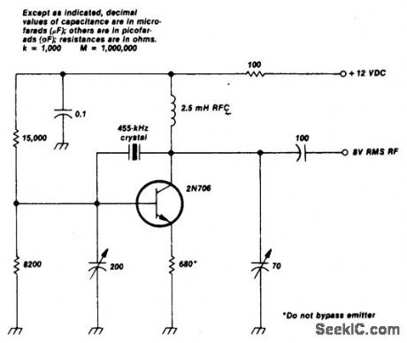
CARRIER_CURRENT_TRANSMITTER_1
Published:2009/6/24 23:25:00 Author:May
View full Circuit Diagram | Comments | Reading(0)
| Pages:1318/2234 At 2013011302130313041305130613071308130913101311131213131314131513161317131813191320Under 20 |
Circuit Categories
power supply circuit
Amplifier Circuit
Basic Circuit
LED and Light Circuit
Sensor Circuit
Signal Processing
Electrical Equipment Circuit
Control Circuit
Remote Control Circuit
A/D-D/A Converter Circuit
Audio Circuit
Measuring and Test Circuit
Communication Circuit
Computer-Related Circuit
555 Circuit
Automotive Circuit
Repairing Circuit