
Circuit Diagram
Index 1304
CAPACITANCE_MULTIPLIER
Published:2009/6/25 21:09:00 Author:Jessie
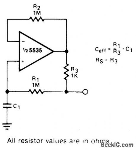
This circuit can be used to simulate large capacitances using small value components. With the values shown and C = 10 μF, an effective capacitance of 10,000 μF was obtained. The Q available is limited by the effective series resistance. So R1 should be as large as practical (View)
View full Circuit Diagram | Comments | Reading(0)
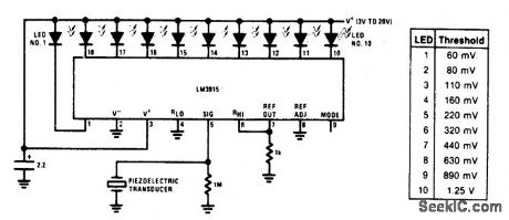
VIBRATION_METER
Published:2009/6/25 20:52:00 Author:May
View full Circuit Diagram | Comments | Reading(0)
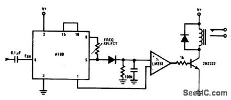
SCA_BACKGROUND_MUSIC_DECODER
Published:2009/6/25 20:52:00 Author:May
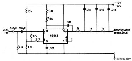
A resistive voltage divider is used to es-tablish a bias voltage for the input (pins 2 and 3). The demodulated (multiplex) FM signal is fed to the input through a two-stage high-pass filter, both to effect capacitive coupling and to attenuate the strong signal o f the regular chan-nel. A total signal amplitude, between 80 mV and 300 mV, is required at the input. Its source should have an impedance of less than 10,000 ohms. The Phase Locked Loop is tuned to 67 kHz with a 5000 ohm potentiometer; only ap-proximate tuning is required, since the loop will seek the signal. The demodulated output (pin 7) passes through a three-stage low-pass filter to provide de-emphasis and attenuate the high-frequency noise which often accompanies SCA transmission. The demodulated output signal is in the rder of 50m V and the frequency response extends to 7 kHz. (View)
View full Circuit Diagram | Comments | Reading(0)
TONE_BURST_GENERATOR
Published:2009/6/25 21:09:00 Author:Jessie
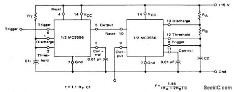
The first timer is used as a monostable and determines the tone duration when triggered by a positive pulse at pin 6. The second timer is enabled by the high output of the monostable. It is connected as an astable and determines the frequency of the tone. (View)
View full Circuit Diagram | Comments | Reading(0)
LINEAR_VARIABLE_DIFFERENTIAL_TRANSFORMER(LVDT)MEASURING_GAUGE
Published:2009/6/25 20:52:00 Author:May
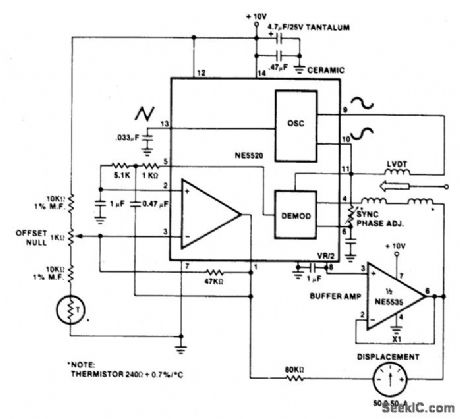
View full Circuit Diagram | Comments | Reading(0)
MUSICAL_ORGAN
Published:2009/6/25 21:07:00 Author:Jessie
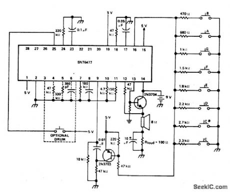
View full Circuit Diagram | Comments | Reading(885)
DOOR_CHIMES_DELAY
Published:2009/6/25 21:06:00 Author:Jessie
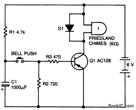
Circuit NotesWith values shown, this simple circuit will permit one operation every 10 seconds or so.Capacitor C1 charges through RI when the button is released. Making RI larger crease the delay. (View)
View full Circuit Diagram | Comments | Reading(1304)
FOUR_CHANNEL_SYNTHESIZER
Published:2009/6/25 21:05:00 Author:Jessie
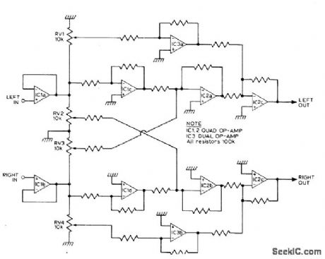
This circuit will synthesize two rear chan-nels for quadraphonic sound when fed with a stereo signal. The rear output for the left chan-nel, is a combination of the left channel input 180 out of phase, added to a proportion of the right hand channel (also out of phase). The right hand rear output is obtained in a similar way. (View)
View full Circuit Diagram | Comments | Reading(1828)
MICROMETRONOME
Published:2009/6/25 21:04:00 Author:Jessie
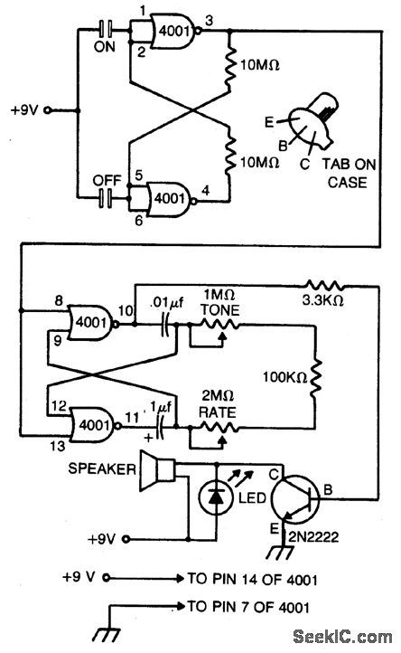
This compact metronome will run for years on a single nine-volt transistor battery.Has both tone and pulse rate controls, and uses touch plates to start and stop, can be built in a case no larger than a pack of cigarettes. The touch plates consist of two strips of metal about 1/16-inch apart mounted on, but insulated from, the case. Bridging the gap closes the switch. (View)
View full Circuit Diagram | Comments | Reading(1261)
LINEAR_VARIABLE_DIFFFERENTIAL_TRANSFORMER(LVDT)DRIVER_DEMODULATOR
Published:2009/6/25 20:51:00 Author:May
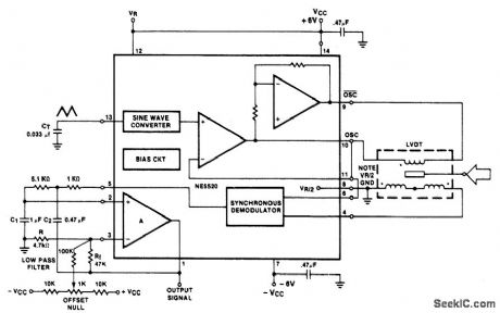
View full Circuit Diagram | Comments | Reading(2611)
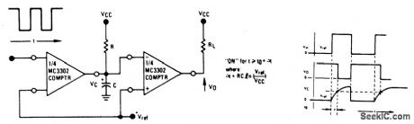
SOUND_LEVEL_MONITOR
Published:2009/6/25 20:50:00 Author:May
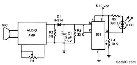
Loudness detector consists of a 555 IC wired as a Schmitt trigger. The output changes state—from high to low—whenever the input crosses a certain voltage. That threshold voltage is established by the setting of R4. (View)
View full Circuit Diagram | Comments | Reading(1400)
STEREO_REVERB_SYSTEM
Published:2009/6/25 21:04:00 Author:Jessie
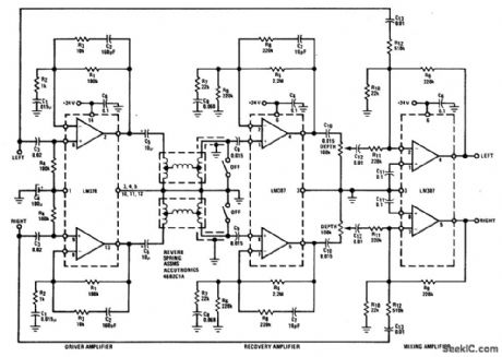
The LM378 dual power amplifier is used as the spring driver. The recovery amplifier is a low noise dual preamplifier. Mixing of the delayed signal with the original is done with another LM387 used in an inverting summing configuration. (View)
View full Circuit Diagram | Comments | Reading(1991)
PEAK_LEVEL_INDICATOR
Published:2009/6/25 20:49:00 Author:May
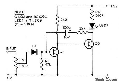
The LED is normally lit, but it will be briefly extinguished if the input exceeds a preset (by RV1) level. A possible application is to monitor the output voltage across a loudspeaker; the LED will flicker with large signals. (View)
View full Circuit Diagram | Comments | Reading(2769)
TONE_DECODER_WITH_RELAY_OUTPUT
Published:2009/6/25 20:48:00 Author:May
View full Circuit Diagram | Comments | Reading(0)
TIME_DELAY_GENERATOR
Published:2009/6/25 21:03:00 Author:Jessie
View full Circuit Diagram | Comments | Reading(0)
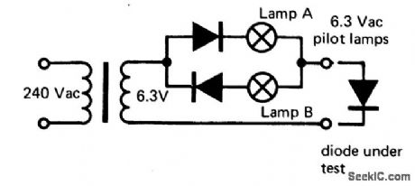
DIODE_TESTER
Published:2009/6/25 20:48:00 Author:May
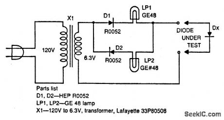
The circuit tests whether or not a diode is open, shorted, or functioning correctly. If lamp A lights, the diode under test is functional. When lamp B is lit, the diode is good but connected backwards. When both lamps are lit, the diode is shamed, and it is open if neither lamp is lit. (View)
View full Circuit Diagram | Comments | Reading(0)
SIGHT_N’SOUND_METRONOME
Published:2009/6/25 21:03:00 Author:Jessie
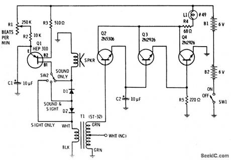
Precise, adjustable control of beats per minute from a largo of 18 to a frenzied, high presto of 500. These beiats are produced acoustically through a speaker. A light flashes at the same rate. When SW1 is closed, C1 begins to charge through R1 and R2. C1 will eventually reach a voltage at which the emitter of unijunction transistor is switched on, dumping the energy stored in C1 into an 8 ohm speaker. To produce a distinct plop , brief pulses across T2 secondary drive Q2 into conduction. The extra gain of Q3 and Q4 are sufficient to briefly switch L1 on, then off, as the pulse wave passes. Capacitor C2 stretches the pulse slightly to overcome the thermal inertia of the lamp, so that a bright flash occurs. (View)
View full Circuit Diagram | Comments | Reading(1203)
GO/NO_GO_DIODE_TESTER
Published:2009/6/25 20:46:00 Author:May
If lamp A or B is illuminated, the diode is serviceable. If both light, the diode is short circuited. If neither light, diode is an open circuit. (View)
View full Circuit Diagram | Comments | Reading(736)
LONG_TIME_DELAY
Published:2009/6/25 21:02:00 Author:Jessie
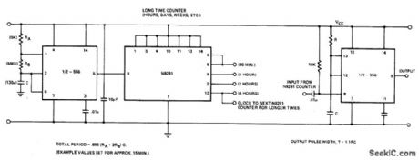
Circuit NotesIn the 556 timer, the timing is a function of the charging rate of the external capacitor. For long time delays, expensive capacitors with extremely low leakage are required. The prac-ticality of the components involved limits the time between pulses to something in the neighborhood of 10 minutes. To achieve longer time periods, both halves of a dual timer may be connected in tandem with a Divide-by ' net-work in between the first timer section oper-ates in an oscillatory mode with a period of 1/fo. This signal is then applied to a Divide-by-N network to give an output with the period of N/fo. This can then be used to trigger the second half of the 556. The total time delay is now a function of N and fo. (View)
View full Circuit Diagram | Comments | Reading(1687)
PHASE_METER
Published:2009/6/25 20:55:00 Author:Jessie

View full Circuit Diagram | Comments | Reading(1219)
| Pages:1304/2234 At 2013011302130313041305130613071308130913101311131213131314131513161317131813191320Under 20 |
Circuit Categories
power supply circuit
Amplifier Circuit
Basic Circuit
LED and Light Circuit
Sensor Circuit
Signal Processing
Electrical Equipment Circuit
Control Circuit
Remote Control Circuit
A/D-D/A Converter Circuit
Audio Circuit
Measuring and Test Circuit
Communication Circuit
Computer-Related Circuit
555 Circuit
Automotive Circuit
Repairing Circuit