
Circuit Diagram
Index 1312
WIDE_RANGE_CURRENT_TO_FREQUENCY_CONVERTER
Published:2009/6/25 2:19:00 Author:May
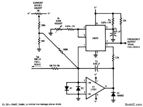
View full Circuit Diagram | Comments | Reading(985)
22_WATT_INCANDESCENT_LAMP_DRIVER
Published:2009/6/25 2:18:00 Author:May
View full Circuit Diagram | Comments | Reading(634)
SHIFT_REGISTER
Published:2009/6/25 2:17:00 Author:Jessie
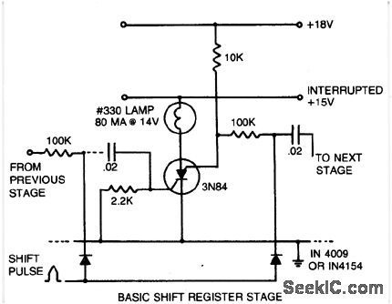
The shift pulse amplitude is less than 15 volts. If a stage is off,the shift pulse will not becoupled to the next stage,If it is on,the diode will conduct and trigger the next stage.Just prior to the shift pulse the anode supply is interrupted to turn off all stages.The stored capacitor charge determines which stages will be triggered, (View)
View full Circuit Diagram | Comments | Reading(0)
HIGH_IMPEDANCE_PRECISION_RECTIFIER_FOR_AC_DC_CONVERTER
Published:2009/6/25 2:18:00 Author:May
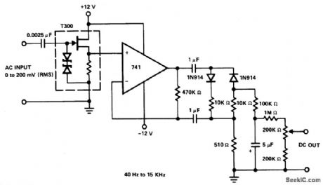
View full Circuit Diagram | Comments | Reading(761)
SHIFT_REGISTER
Published:2009/6/25 2:17:00 Author:May
The shift pulse amplitude is less than 15 volts. If a stage is off,the shift pulse will not becoupled to the next stage,If it is on,the diode will conduct and trigger the next stage.Just prior to the shift pulse the anode supply is interrupted to turn off all stages.The stored capacitor charge determines which stages will be triggered, (View)
View full Circuit Diagram | Comments | Reading(0)
POWER_VOLTAGE_TO_CURRENT_CONVERTER
Published:2009/6/25 2:17:00 Author:May
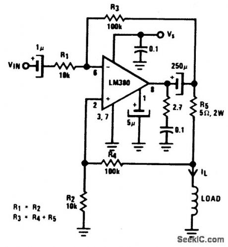
Low cost converter is capable of supplying constant ac currents up to 1 A over variable loads. (View)
View full Circuit Diagram | Comments | Reading(0)
BUTLER_COMMON_BASE_OSCILLATOR_BASIC_CIRCUIT
Published:2009/6/25 2:17:00 Author:May
Circuit Notes This circuit operates at or near series resonance. It has fair to poor circuit design with parasitics, touch to tune, and fair frequency stability. (View)
View full Circuit Diagram | Comments | Reading(0)
CALCULATOR_TO_STOPWATCH_CONVERTER
Published:2009/6/25 2:17:00 Author:May
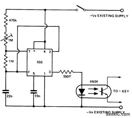
This circuit can be fitted to any calculator existing with an automatic constant to enable it to be used as a stop-watch. The 555 timer is set to run at a suitable frequency and connected to the existing calculator battery via the push-on push-off switch and the existing calculator on-off switch. (View)
View full Circuit Diagram | Comments | Reading(0)
BATTERY_LANTERN_CIRCUIT_
Published:2009/6/25 2:15:00 Author:May
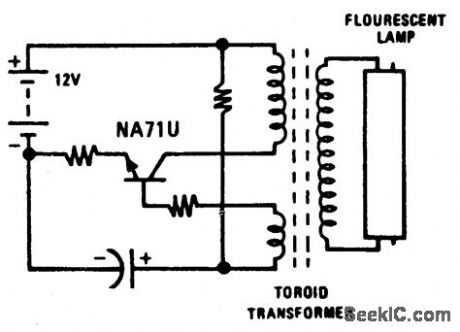
View full Circuit Diagram | Comments | Reading(1134)
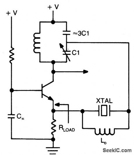
COLPITTS_HARMONIC_OSCILLATOR(BASIC_CIRCUIT)
Published:2009/6/25 2:14:00 Author:May
Circuit NotesThis circuit operates 30-200 ppm above series resonance. Physically simple, but analytically complex. It is inexpensive with fair frequency stability. (View)
View full Circuit Diagram | Comments | Reading(0)
POWER_VOLTAGE_TO_CURRENT_CONVERTER
Published:2009/6/25 2:17:00 Author:Jessie
Low cost converter is capable of supplying constant ac currents up to 1 A over variable loads. (View)
View full Circuit Diagram | Comments | Reading(1310)
BUTLER_EMITTER_FOLLOWER_OSCILLATOR(100_MHz)
Published:2009/6/25 2:13:00 Author:May
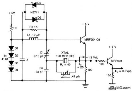
Circuit NotesThis circuit has good performance without any parasitics because emitter follower amplifier has a gain of only one with built-in negative feedback to stabilize its gain. (View)
View full Circuit Diagram | Comments | Reading(1328)
BUTLER_COMMON_BASE_OSCILLATOR_BASIC_CIRCUIT
Published:2009/6/25 2:17:00 Author:Jessie
Circuit Notes This circuit operates at or near series resonance. It has fair to poor circuit design with parasitics, touch to tune, and fair frequency stability. (View)
View full Circuit Diagram | Comments | Reading(1618)
CURRENT_TO_VOLTAGE_CONVERTER
Published:2009/6/25 2:12:00 Author:May
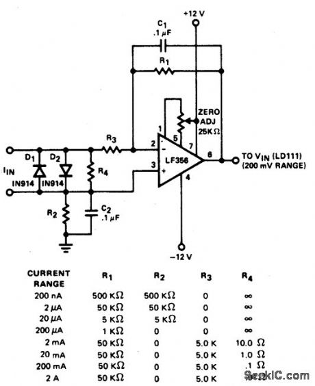
Converter features eight decades of cur-rent range. The circuit is intended to be used with the 200.0 mV range of a DVM. (View)
View full Circuit Diagram | Comments | Reading(0)
COMPLEMENTARY_AC_POWER_SWITCHING
Published:2009/6/25 2:11:00 Author:May
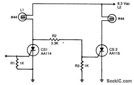
An input signal of less than 1 mA and 1 V is required to switch on CS1. As long as this input signal is maintained, CS1 will conduct during each positive half cycle of anode voltage, thereby energizing load L1 with half-wave rectified dc. L2 remains de-energized, since the anode of CS1 will not go more positive than 1.5 volts, and voltage divider R2 - R3 cannot provide enough voltage to trigger CS2. Upon removal of the input signal, CS1 will drop out.L1 will be de-energized, except for a small amount of ac current through R2 and R3. CS2will be triggered on at the beginning of each positive half-cycle, when CS1 anode voltage reaches 2 to 3 volts. CS2 will conduct for nearly the entire positive half-cycle energizing L2. It should be noted that the 6.3 volt lamps used will operate at 1/3 the rated brilliance because of the controlled switch half-wave rectifying action and will extend the operating lamp life by several orders of magnitude. Should full brilliance be desired, the anode supply voltage level should be raised to 9 volts ac. (View)
View full Circuit Diagram | Comments | Reading(0)
CALCULATOR_TO_STOPWATCH_CONVERTER
Published:2009/6/25 2:17:00 Author:Jessie
This circuit can be fitted to any calculator existing with an automatic constant to enable it to be used as a stop-watch. The 555 timer is set to run at a suitable frequency and connected to the existing calculator battery via the push-on push-off switch and the existing calculator on-off switch. (View)
View full Circuit Diagram | Comments | Reading(2844)
HI_LO_RESISTANCE_TO_VOLTAGE_CONVERTER
Published:2009/6/25 2:10:00 Author:May
View full Circuit Diagram | Comments | Reading(808)
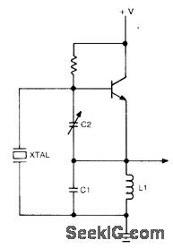
BUTLER_EMITTER_FOLLOWER_OSCILLATOR_BASIC_CIRCUIT
Published:2009/6/25 2:16:00 Author:Jessie
Circuit Notes
This circuit operates at or near series resonance. It is a good circuit design with no parasitics. It is easy to tune with good fre-quency stability. (View)
View full Circuit Diagram | Comments | Reading(683)
LOW_COST,μP_INTERFACED,TEMPERATURE_TO_DIGITAL_CONVERTER
Published:2009/6/25 2:09:00 Author:May
View full Circuit Diagram | Comments | Reading(748)
LIGHT_LEVEL_CONTROLLER
Published:2009/6/25 2:16:00 Author:Jessie
View full Circuit Diagram | Comments | Reading(620)
| Pages:1312/2234 At 2013011302130313041305130613071308130913101311131213131314131513161317131813191320Under 20 |
Circuit Categories
power supply circuit
Amplifier Circuit
Basic Circuit
LED and Light Circuit
Sensor Circuit
Signal Processing
Electrical Equipment Circuit
Control Circuit
Remote Control Circuit
A/D-D/A Converter Circuit
Audio Circuit
Measuring and Test Circuit
Communication Circuit
Computer-Related Circuit
555 Circuit
Automotive Circuit
Repairing Circuit