
Circuit Diagram
Index 1294
AUTOMATIC_PLANT_WATERER
Published:2009/6/25 22:35:00 Author:Jessie
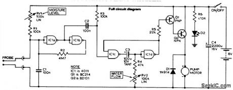
The unit consists of a sensor, timer, and electric water pump. The sensor is embedded in the soil, and when dry, the electronics operate the water pump for a preset time. The circuit is composed of a level sensitive Schmitt trigger, variable time monostable, and output driver. When the resistance across the probe increases beyond a set value (i.e., the soil dries), the Schmitt is triggered. C2 feeds a negative going pulse to the monostable when the Schmitt triggers and R2 acts as feedback, to ensure a fast switching action. (View)
View full Circuit Diagram | Comments | Reading(2060)
AUTOMATIC_PLANT_WATERER
Published:2009/6/25 22:35:00 Author:May
The unit consists of a sensor, timer, and electric water pump. The sensor is embedded in the soil, and when dry, the electronics operate the water pump for a preset time. The circuit is composed of a level sensitive Schmitt trigger, variable time monostable, and output driver. When the resistance across the probe increases beyond a set value (i.e., the soil dries), the Schmitt is triggered. C2 feeds a negative going pulse to the monostable when the Schmitt triggers and R2 acts as feedback, to ensure a fast switching action. (View)
View full Circuit Diagram | Comments | Reading(0)
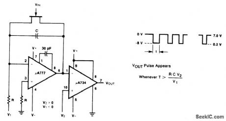
PULSE_WIDTH_DISCRIMINATOR
Published:2009/6/25 22:34:00 Author:Jessie
View full Circuit Diagram | Comments | Reading(0)
PULSE_WIDTH_DISCRIMINATOR
Published:2009/6/25 22:34:00 Author:May
View full Circuit Diagram | Comments | Reading(0)
ULTRA_LOW_DRIFT_PEAK_DETECTOR
Published:2009/6/25 22:33:00 Author:Jessie
View full Circuit Diagram | Comments | Reading(2143)
ULTRA_LOW_DRIFT_PEAK_DETECTOR
Published:2009/6/25 22:33:00 Author:May
View full Circuit Diagram | Comments | Reading(0)
MOISTURE_DETECTOR
Published:2009/6/25 22:32:00 Author:Jessie
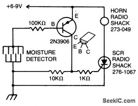
The detector is made of fine wires spaced about one or two inches apart. When the area between a pair of wires becomes moistened, the horn will sound. To turn it off, dc power must be disconnected. (View)
View full Circuit Diagram | Comments | Reading(0)
RAIN_ALARM
Published:2009/6/25 22:31:00 Author:Jessie
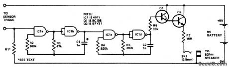
The circuit uses four NAND gates of a 4011 package. In eachoscillator, while one gate is configured as a straightforward inverter, the other has one input that can act as a control input. Oscillator action is inhibited if this input is held low. The first oscillator (IC1a and IC1b) has this input tied low via a high value resistor (R1) that acts as a sensitivity control. Thus this oscillator will be disabled until the control input is taken high. Any moisture bridging the sensor track will so enable the output which is a square wave at about 10 Hz. This in turn will gate on and off the 500 Hz oscillator formed by IC1c and IC1d. This latter oscillator drives the loudspeaker via R6, the Darlington pair formed by Q1 and Q2, and resistor R7. (View)
View full Circuit Diagram | Comments | Reading(0)
MOISTURE_DETECTOR
Published:2009/6/25 22:32:00 Author:May
The detector is made of fine wires spaced about one or two inches apart. When the area between a pair of wires becomes moistened, the horn will sound. To turn it off, dc power must be disconnected. (View)
View full Circuit Diagram | Comments | Reading(0)
EDGE_DETECTOR
Published:2009/6/25 22:31:00 Author:Jessie
Circuit Notes
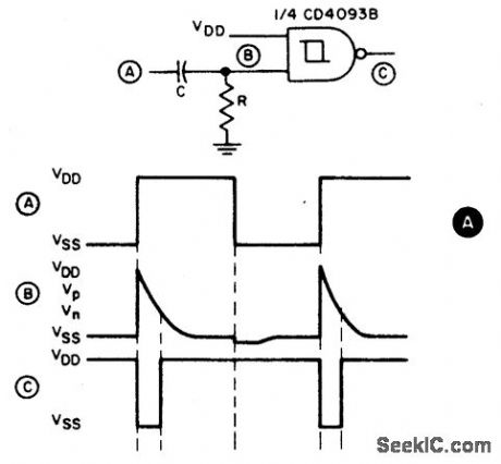
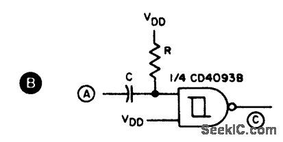
This circuit provides a short negativegoing output pulse for every positive-going edge at the input. The input waveform is coupled to the input by capacitor C; the pulse O length denends, as before, on R and C. If a negattve gomg edge detector is required, the circuit in B should be used. (View)
View full Circuit Diagram | Comments | Reading(5106)
WIDEBAND_BUFFER
Published:2009/6/25 22:31:00 Author:May
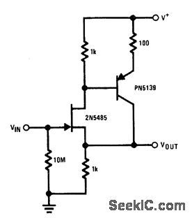
Low input capacitance of 2N5485 FET makes compound series-feedback buffer serve as wideband unity-gain amplifier having high input impedance.- FET Data-book, National Semiconductor, Santa Clara,CA,1977, p 6-26-6-36. (View)
View full Circuit Diagram | Comments | Reading(2393)
RAIN_ALARM
Published:2009/6/25 22:31:00 Author:May
The circuit uses four NAND gates of a 4011 package. In eachoscillator, while one gate is configured as a straightforward inverter, the other has one input that can act as a control input. Oscillator action is inhibited if this input is held low. The first oscillator (IC1a and IC1b) has this input tied low via a high value resistor (R1) that acts as a sensitivity control. Thus this oscillator will be disabled until the control input is taken high. Any moisture bridging the sensor track will so enable the output which is a square wave at about 10 Hz. This in turn will gate on and off the 500 Hz oscillator formed by IC1c and IC1d. This latter oscillator drives the loudspeaker via R6, the Darlington pair formed by Q1 and Q2, and resistor R7. (View)
View full Circuit Diagram | Comments | Reading(3681)
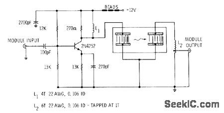
CASCODE_RF_IF
Published:2009/6/25 22:31:00 Author:May
Uses half of SignetIcs 511 transistor array to provide voltage gain of about 10 over bandwidth of 2 MHz with output volt-age swing of 12V P-P. Design procedure is given. Circuit provides excellent isolation be-tween input and output.- Signetics Analog Data Manual, Signetics, Sunnyvale, CA,1971, p 746-747. (View)
View full Circuit Diagram | Comments | Reading(760)
EDGE_DETECTOR
Published:2009/6/25 22:31:00 Author:May
Circuit Notes
This circuit provides a short negativegoing output pulse for every positive-going edge at the input. The input waveform is coupled to the input by capacitor C; the pulse O length denends, as before, on R and C. If a negattve gomg edge detector is required, the circuit in B should be used. (View)
View full Circuit Diagram | Comments | Reading(0)
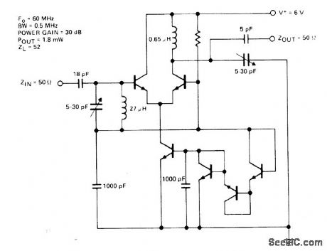
168_MHz_BANDPASS
Published:2009/6/25 22:31:00 Author:May
Gain stage provides gain of 6 dB from 162 to 174 MHz. Skirt slope immediately outside passband decreases at 80 db/MHz. Uses dispersive-design surface-acous-tic-wave bandpass filter with 168-MHz center frequency, 7% bandwidth, and extremely steep skirt response. Parallel inductor at collector ter-minal matches capacitance of acoustic-wave device, and tapped inductor matches output terminal of filter to 50 ohms. Used in spread-spectrum communication receiver. Article cov-ers design and construction of filter on quartz substrate.-T.F.Cheek, Jr.,R.M.Hays,Jr.,and C.S.Hartmann, A Wide-Band Low-Shape-Fac-tor Amplifier Module Using an Acoustic Sur-face-Wave Bandpass Filter, IEEE Joumal of Solid-State Circuits, Feb. 1973, p 66-70. (View)
View full Circuit Diagram | Comments | Reading(728)
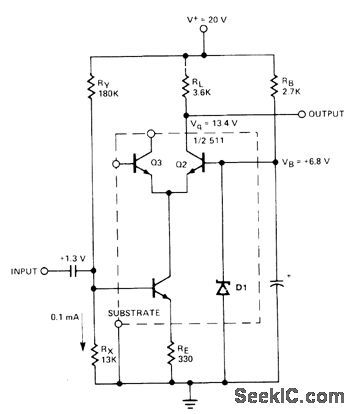
60_MHz_NARROW_BAND
Published:2009/6/25 22:30:00 Author:May
Signetics NE510/511 transistor array provides bandwidth of 0.5 MHz for 3dB down and noise figure of 7 dB for power gain of 30dB,Maximum output swing across 50 ohms is 300 mVRMS. Circuit is easily tuned.- Signetics Analog Data Manual. Signetics, Sunnyvale, CA,1977, p 749. (View)
View full Circuit Diagram | Comments | Reading(739)
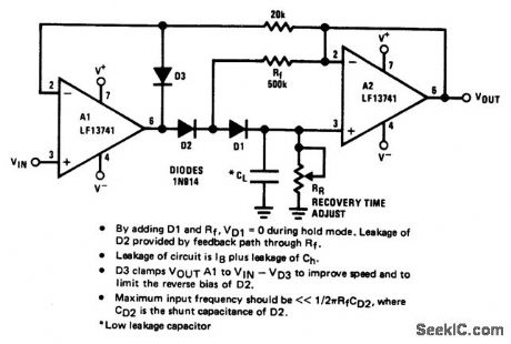
PRECISION_PEAK_VOLTAGE_DETECTOR_WITH_A_LONG_MEMORY_TIME
Published:2009/6/25 22:29:00 Author:May


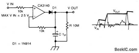
Circuit Notes
The circuit has negative feedback only for positive signals. The inverting input can only get some feedback when diode Dl is forward biased and only occurs when the input is posi-tive. With a positive input signal, the output of the op amp rises until the inverting input signal reaches the same potential. In so doing, the capacitor C is also charged to this potential.When the input goes negative, the diode Dl becomes reverse biased, the voltage on the capacitor remains, being slowly discharged by the op amp input bias current of 10 pico amps.Thus the discharge of the capacitor is domin-antly controlled by the resistor R, giving a time constant of 10 seconds. Thus, the circuit de-tects the most positive peak voltage and remembers it. (View)
View full Circuit Diagram | Comments | Reading(0)
TELEPHONE_OFF_HOOk_INDICATOR
Published:2009/6/25 22:27:00 Author:May
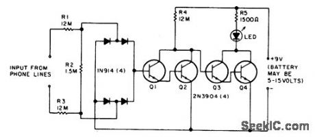
The LED flickers when the phone is ringing or being dialed. It glows steadily when the phone is off the hook. (View)
View full Circuit Diagram | Comments | Reading(1474)
TELEPHONE_LINE_POWERED_REPERTORY_DIALER
Published:2009/6/25 22:26:00 Author:May
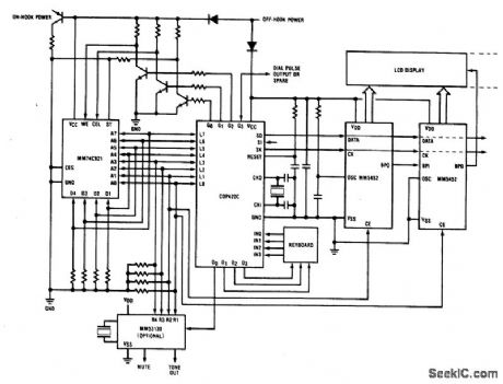
Repertory dialer phone has a library of fifteen frequently used numbers,(plus the last number dialed)stored In a standard CMOS RAM,A pushbutton keyboardenables telephone numbers to be keyed in and dialed out directly or a telephone number to be stored in the RAM and dialed automatically. (View)
View full Circuit Diagram | Comments | Reading(729)
70_dB_VOLTAGECONTROLLED_GAIN
Published:2009/6/25 22:24:00 Author:May
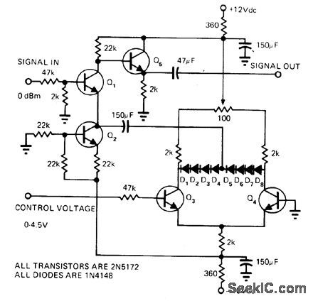
Amplifier Q1 uses current source Q2 as emitter resistor to provide correct current bias for class A operation. Coupling through 150-μF capacitor to silicon diode string D1-D8 provides variable re-sistance needed to achieve variable gain. Sim-ple differential amplifier Q3-Q4 adjusts forward bias of diodes to change their forward resis-tanco. Increasing positive control voltage from 0 to 4.5 V changes voltage gain from -74 dBm to about -4 dBm with respect to 0-dBm input signaL-N.A Steiner, Voltage-Controlled Am-plifier Covers 70 dB Range, EDN Magazine, March 5, 1975, p 72 and 74. (View)
View full Circuit Diagram | Comments | Reading(698)
| Pages:1294/2234 At 2012811282128312841285128612871288128912901291129212931294129512961297129812991300Under 20 |
Circuit Categories
power supply circuit
Amplifier Circuit
Basic Circuit
LED and Light Circuit
Sensor Circuit
Signal Processing
Electrical Equipment Circuit
Control Circuit
Remote Control Circuit
A/D-D/A Converter Circuit
Audio Circuit
Measuring and Test Circuit
Communication Circuit
Computer-Related Circuit
555 Circuit
Automotive Circuit
Repairing Circuit