
Circuit Diagram
Index 1295
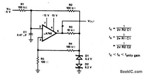
PRECISION_PEAK_VOLTAGE_DETECTOR_WITH_A_LONG_MEMORY_TIME
Published:2009/6/25 22:29:00 Author:Jessie


Circuit Notes
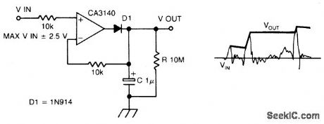
The circuit has negative feedback only for positive signals. The inverting input can only get some feedback when diode Dl is forward biased and only occurs when the input is posi-tive. With a positive input signal, the output of the op amp rises until the inverting input signal reaches the same potential. In so doing, the capacitor C is also charged to this potential.When the input goes negative, the diode Dl becomes reverse biased, the voltage on the capacitor remains, being slowly discharged by the op amp input bias current of 10 pico amps.Thus the discharge of the capacitor is domin-antly controlled by the resistor R, giving a time constant of 10 seconds. Thus, the circuit de-tects the most positive peak voltage and remembers it. (View)
View full Circuit Diagram | Comments | Reading(2053)
SUMMING_AMPLIFIER
Published:2009/6/25 22:23:00 Author:May
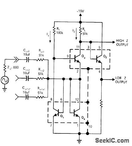
Uses RCA CA3018 four-transistor array as current-mirror triad with low 4 mpedance buffered output, to serve as high-performance summing amplifier. Mea-sured harmonic distortion is less than 170 at voltage gains up to 50 and with output swing of 10V P-P. High output impedance of 51 kil-ohms can be buffered by Q2 connected as emitter-follower.-W.G.Jung. Monolithic-Triad Cument Summer, EDNIEEE Magazine, July 1,1971,p52. (View)
View full Circuit Diagram | Comments | Reading(1489)
FET_CASCODE_VIDEO
Published:2009/6/25 22:22:00 Author:May
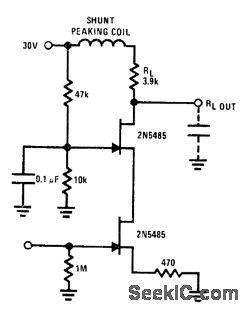
Use of 2N5485 FETs gives very low input loading, with feedback reduced almostto zero,Bandwidth of amplifier is limited only by load resistance and capacitance.-″FET Databook,″ National Semiconductor,Santa Clara,CA,1977、p 6-26-6-36 (View)
View full Circuit Diagram | Comments | Reading(766)
40_265_MHz_VMOS
Published:2009/6/25 22:21:00 Author:May
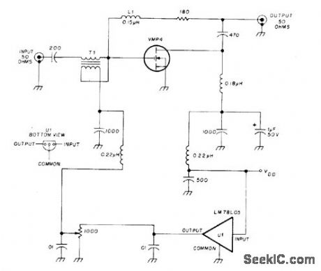
Wideband power amplifier using Siliconix Mospower FET in negative-feed-back circuit has flat gain within 0.5 dB over entire operational range of 40 to 265 MHz. Use 6 to 8 turns of No.30 on 1/2-W 1-megohm resistor for L1 (not commercially molded choke). T1 is 4 turns No.22 twisted- pair on Indiana General F625-902 toroid core. Avoid static charges until transistor is soldered into circuit.-E. Oxner, Mospower FET as a Broadband Amplifier, Ham Radlio, Dec.1976, p 32-35. (View)
View full Circuit Diagram | Comments | Reading(711)
TELEPHONE_CONTROLLED_TAPE_STARTER_TCTS
Published:2009/6/25 22:18:00 Author:May
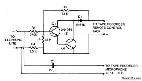
This circuit converts a tape recorder into a completely automatic telephone conversation recording instrument that needs no external power source. Voltage at the switch terminals of tape recorder applied to a pair of Darlington-connected transistors, Q1 and Q2, will turn on and start the tape recorder. To turn the transistors off, and thereby stop the machine, apply a negative voltage to the base of Q1 from the phone line. When the telephone receiver is on the hook, there is typically about 50 volts dc across the phone divided across R1, R2, and R4 in such a way that the base of Q1 is sufficiently negative to keep the tape recorder off. When the phone's receiver is picked up, the voltage on the telephone line drops to about 5 volts, which leaves insufficient negative vol-tage on the base of Q1 to keep it cut off, so the tape recorder starts and begins to record. (View)
View full Circuit Diagram | Comments | Reading(807)
VHF_MODULATOR
Published:2009/6/25 22:17:00 Author:May
View full Circuit Diagram | Comments | Reading(0)
TELEPHONE_RELAY
Published:2009/6/25 22:17:00 Author:May
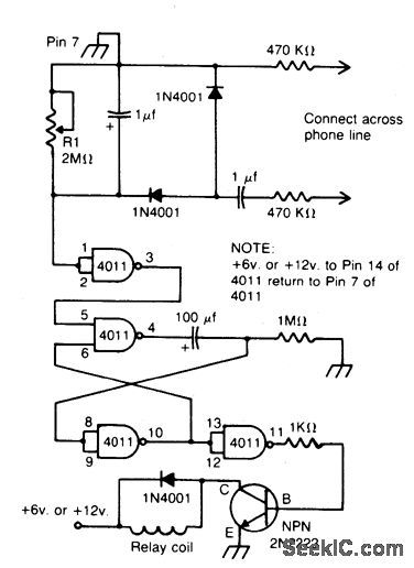
Connected across the bell circuit of phone, this circuit closes a relay when the phone is ringing. Use the delay contacts to actuate any bell, siren, buzzer or lamp. (View)
View full Circuit Diagram | Comments | Reading(1154)
TONE_DIAL_DECODER
Published:2009/6/25 22:16:00 Author:May
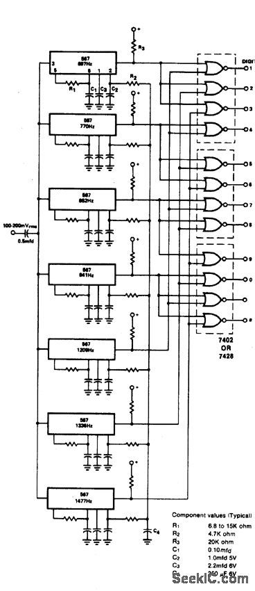
View full Circuit Diagram | Comments | Reading(647)
TELEPHONE_OFF_HOOk_INDICATOR
Published:2009/6/25 22:27:00 Author:Jessie
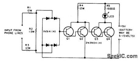
The LED flickers when the phone is ringing or being dialed. It glows steadily when the phone is off the hook. (View)
View full Circuit Diagram | Comments | Reading(0)
4PULSE_WIDTH_MODULATOR
Published:2009/6/25 22:16:00 Author:May
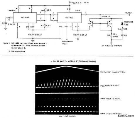
View full Circuit Diagram | Comments | Reading(727)
REMOTE_RING_EXTENDER_SWITCH
Published:2009/6/25 22:15:00 Author:May
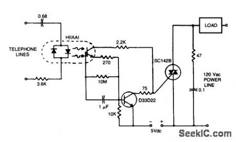


The circuit can operate lamps and buzzers from the 120V, 60 Hz power line while main-taining positive isolation between the tele-phone line and the power line. Use of the iso-lated tab triac simplifies heat sinking by removing the constraint of isolating the triac heat sink from the chassis. (View)
View full Circuit Diagram | Comments | Reading(791)
3PULSE_WIDTH_MODULATOR
Published:2009/6/25 22:14:00 Author:May
View full Circuit Diagram | Comments | Reading(644)
TONE_DIAL_SEQUENCE_DECODER
Published:2009/6/25 22:14:00 Author:May
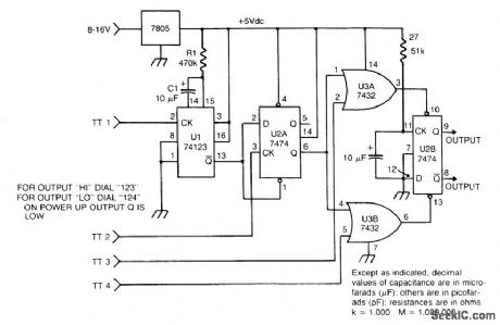
The circuit takes active low inputs from a Touch Tone decoder and reacts to a proper sequence of digits. The proper sequence is determined by which Touch Tone digits the user connects to the sequence decoder inputs TT1, TT2, TT3, and TT4. (View)
View full Circuit Diagram | Comments | Reading(1010)
TV_MODULATOR_USING_A_MOTOROLA_MC1374
Published:2009/6/25 22:13:00 Author:May
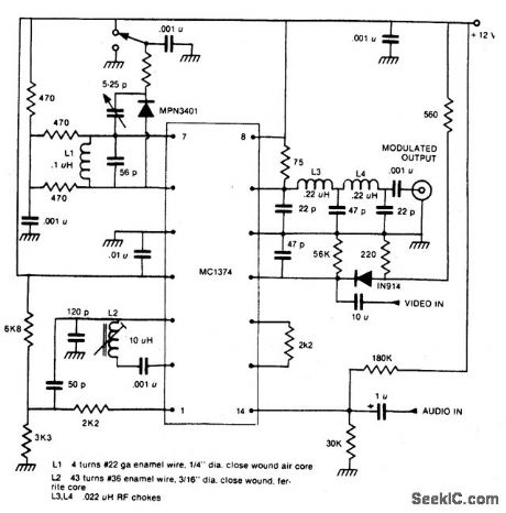
This one-chip modulator requires some outboard circuitry and a shielded box. (View)
View full Circuit Diagram | Comments | Reading(1258)
TONE_DIAL_ENCODER
Published:2009/6/25 22:13:00 Author:May
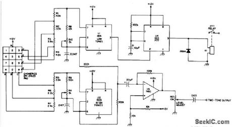
Tone dial encoder with automatic PTT control uses the 555 timers. (View)
View full Circuit Diagram | Comments | Reading(817)
TONE_DIAL_GENERATOR
Published:2009/6/25 22:12:00 Author:May
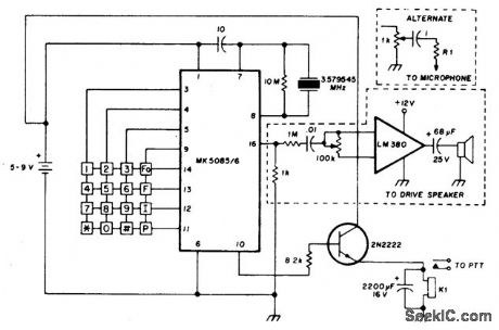
The circuit requires a minimum of parts and uses a low cost standard 3.579545-MHz television color-burst crystal. The speaker can be eliminated and the output fed directly into the microphone input of a transmitter. (View)
View full Circuit Diagram | Comments | Reading(945)
AM_MODULATOR
Published:2009/6/25 22:11:00 Author:May
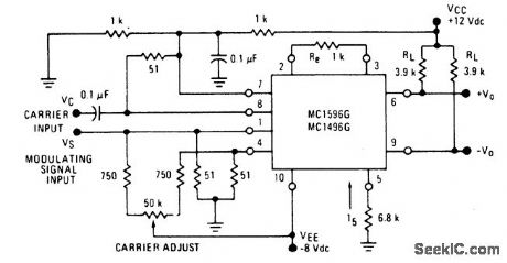
View full Circuit Diagram | Comments | Reading(863)
2PULSE_WIDTH_MODULATOR
Published:2009/6/25 22:10:00 Author:May
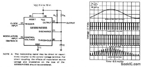
The monostable circuit is triggered by a continuous input pulse train and the threshold voltage is modulated by a control signal. The resultant effect is a modulation of the output pulse width, as shown. A sine-wave modulation signal is illustrated, but any wave-shape could be used. (View)
View full Circuit Diagram | Comments | Reading(907)
RC_COUPLED_DIFFERENTIAL
Published:2009/6/25 22:10:00 Author:May
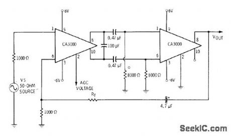
Input signal is applied to base of first differential amplifier and pushpull output is obtained from pins 8 and 10 for transfer to inputs of second IC. Feedback is transferred through RC combination back to pin 6 of first IC. Gain is varied with AGO voltage ap-plied to pin 2 of first IC. Gain is over 60 dB with flat response from 100 Hz to 100 kHz.-E.M.Noll, Linear IC Principles, Experiments, and Projects, Howard W. Sams, Indianapolis, IN, 1974, p 89-91. (View)
View full Circuit Diagram | Comments | Reading(826)
25_MHz_BANDWIDTH_LOW__NOISE
Published:2009/6/25 22:09:00 Author:May
RCA CA3018 fourtransistor array is connected as two pairs of common-emitter emitter-follower combinations, with two feedback loops providing high DC stabilhy. One path goes from emitter of Q3 back to input, and other goes from collector of Q4 to collector of Q1. Values of C1, C2, and C3 give low-frequency cutoff (3 dB down) of 800 Hz.Upper cutoff is 32 MHz.-E.M.Noll, Linear IC Principles, Experiments, and Projects, Howard W. Sams, Indianapolis, IN,1974, p 165-168 and 174. (View)
View full Circuit Diagram | Comments | Reading(826)
| Pages:1295/2234 At 2012811282128312841285128612871288128912901291129212931294129512961297129812991300Under 20 |
Circuit Categories
power supply circuit
Amplifier Circuit
Basic Circuit
LED and Light Circuit
Sensor Circuit
Signal Processing
Electrical Equipment Circuit
Control Circuit
Remote Control Circuit
A/D-D/A Converter Circuit
Audio Circuit
Measuring and Test Circuit
Communication Circuit
Computer-Related Circuit
555 Circuit
Automotive Circuit
Repairing Circuit