
Circuit Diagram
Index 1284
100_W_PEP_420_450_MHz_PUSH_PULL_LINEAR_AMPLIFIER
Published:2009/6/26 4:10:00 Author:Jessie
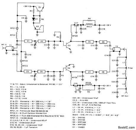
This 100 watt linear amplifier may be constructed using two MRF309 transistors in push-pull, requiring only 16 watts drive from 420 to 450 MHz. Operating from a 28 volt supply, eight dB of power gain is achieved alongwithexcellent practical performance featuring: maximum input SWR of 2:1, har-monic suppression more than-63 dB below 100 watts output, efficiency greater than 40%, circuit stability with a 3:1 collector mismatch at all phase angles. (View)
View full Circuit Diagram | Comments | Reading(912)
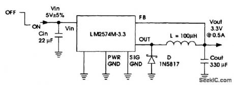
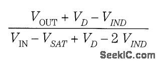
24_V_TO_33_V_SWITCHING_REGULATOR
Published:2009/6/26 4:08:00 Author:Jessie
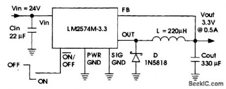
The National Semiconductor LM2574 delivers 3.3 V out at O.SAfrom a 24-V source. The duty cycle is:VD = diode drop(0.39)VIND = inductor dc dropVSAT = saturation voltage of LM2574(0.9 V typical) (View)
View full Circuit Diagram | Comments | Reading(1426)
VLF_CONVERTER
Published:2009/6/26 3:51:00 Author:May
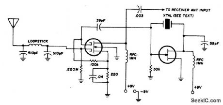
This converter uses a low-pass filter instead of the usual tuned circuit so the only tuning required is with the receiver. The dual-gate MOSFET and FET used in the mixer and oscillator aren't critical. Any crystal having a frequency compatible with the receiver tuning range may be used. For example, with a 3500 kHz crystal, 3500 kHz on the receiver dial corresponds to zero kHz; 3600 to 100 kHz; 3700 to 200 kHz, etc. (At 3500 khz on the receiver all one can hear is the converter os-cillator, and VLF signals start to come in about 20 kHz higher.) (View)
View full Circuit Diagram | Comments | Reading(0)
AUDIO_CONTINUITY_TESTER
Published:2009/6/26 4:05:00 Author:Jessie
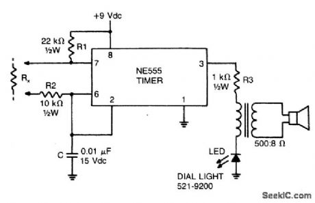
This low-current audio continuity tester indicates the unknown resistance value by the frequency of audio tone. A high tone indicates a low resistance, and a tone of a few pulses per second indicates a resistance as high as 30 megohms. (View)
View full Circuit Diagram | Comments | Reading(1931)
NEON_LAMP_DRIVER_FOR_5_TO_15_V_SUPPLIES
Published:2009/6/26 3:51:00 Author:May
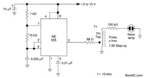
This neon-lamp driver based on the 555 T1 can be wound on an old TV flyback transformer core. (View)
View full Circuit Diagram | Comments | Reading(0)
SQUELCH_CIRCUIT_FOR_AM_OR_FM
Published:2009/6/26 3:50:00 Author:May
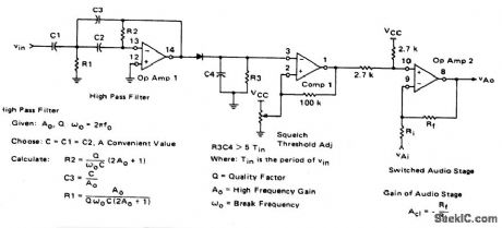
View full Circuit Diagram | Comments | Reading(0)
CURRENT_LIMITING_REGULATOR
Published:2009/6/26 3:49:00 Author:May
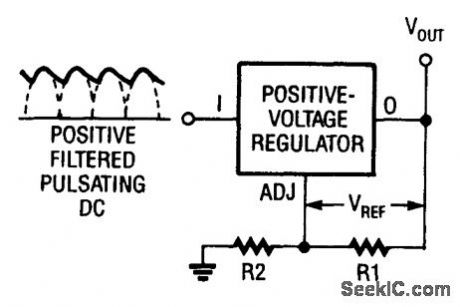
Floating adjustable regulators can be used as current Iimiters. Resistor R1 programs the current flowing through R2. (View)
View full Circuit Diagram | Comments | Reading(0)
5_V_TO_33_V_SWITCHING_REGULATOR
Published:2009/6/26 4:05:00 Author:Jessie
A National Semiconductor LM2574 is used to derive 3.3 V at 0.5 A from a 5-V logic bus. The duty cycle is: VD = diode drop (0.39) VIND = inductor dc drop VSAT = saturation voltage of LM2574 (0.9 V typical) This circuit should be useful to derive 3.3 V for logic devices from existing +5-V buses. (View)
View full Circuit Diagram | Comments | Reading(1346)
LOW_PARTS_COUNT_RATIOMETRIC_RESISTANCE_MEASUREMENT
Published:2009/6/26 4:04:00 Author:Jessie
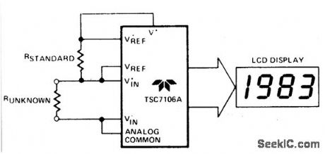
The unknown resistance is put in series with a known standard and a current passed through the pair. The voltage developed across the unknown is applied to the input and the voltage across the known resistor applied to the reference input. If the unknown equals the standard, the display will read 1000. The dis-played reading can be determined from the following expression:Runknown
Displayed Reading= ___________ =×1000 RstandardThe display will overrange for Runknown, ≥2× Rstandard. (View)
View full Circuit Diagram | Comments | Reading(1536)
CMOS_LINE_RECEIVER
Published:2009/6/26 3:45:00 Author:May
The trip point is set half way between the supplies by R1 and R2; R3 provides over 200 mV of hysteresis to increase noise immunity.Maximum frequency of operation is about 300 kHz. If response to TTL levels is desired, change R2 to 39 K. The trip point is now cen-tered at 1.4 V. (View)
View full Circuit Diagram | Comments | Reading(0)
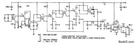
SIMPLE_LF_CONVERTER
Published:2009/6/26 3:44:00 Author:May

This converter allows coverage from 25 kHz up to 500 kHz. Use short coax from the converter to receiver antenna input. Tune the receiver to 3.5 MHz, peak for loudest crystal calibrator and tune your receiver higher in frequency to 3.6 MHz and you're tuning the 100 kHz range. 3.7 MHz puts you at 200 kHz, 3.8 MHz equals 300 kHz, 3.9 MHz yields 500 kHz, and 4.0 MHz gives you 500 kHz. (View)
View full Circuit Diagram | Comments | Reading(0)
FM_RADIO
Published:2009/6/26 3:43:00 Author:May
View full Circuit Diagram | Comments | Reading(0)
ANALOG_RECEIVER_LOW_TEMPERATURE_DRIFT
Published:2009/6/26 3:41:00 Author:May
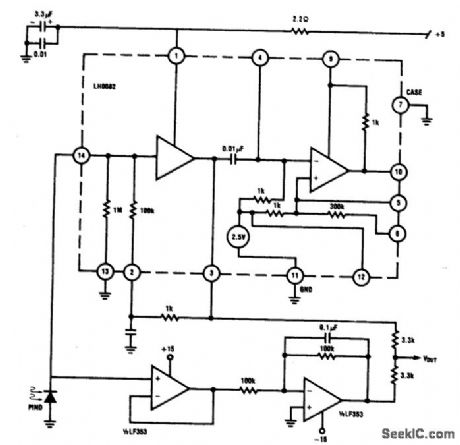
View full Circuit Diagram | Comments | Reading(0)
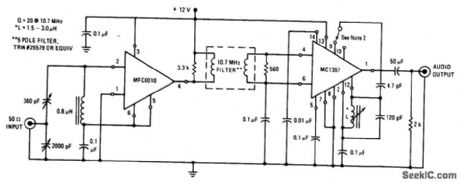
FM_STEREO_DEMODULATION_SYSTEM
Published:2009/6/26 3:40:00 Author:May
View full Circuit Diagram | Comments | Reading(715)
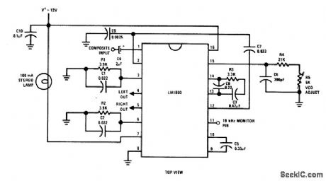
AM_RADIO
Published:2009/6/26 3:39:00 Author:May
View full Circuit Diagram | Comments | Reading(4)
INDUCTORLESS_POWER_SUPPLY_CONVERTER
Published:2009/6/26 3:39:00 Author:May
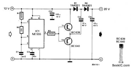
Using a 555 timer and voltage doubler, this circuit will supply ≥50mA at 20 Vdc. T1 and T2 act as power amplifiers to drive the voltage doubler. Frequency of operation is approximately 8.5 kHz. (View)
View full Circuit Diagram | Comments | Reading(3451)
AM_FM_CLOCK_RADIO
Published:2009/6/26 3:38:00 Author:May
View full Circuit Diagram | Comments | Reading(849)
HV_POWER_SUPPLY_WITH_9_TO_15_Vdc_INPUT_
Published:2009/6/26 3:38:00 Author:May
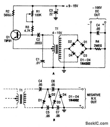
The combination Hartley oscillator/step-up transformer shown in A can generate significant negative high voltage, especially if the voltage output of the transformer is multiplied by the circuit in B. (View)
View full Circuit Diagram | Comments | Reading(756)
COMBINATION_VOLTAGE_AND_CURRENT_REGULATOR
Published:2009/6/26 3:35:00 Author:May
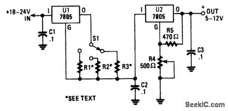
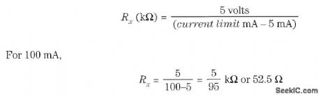
This voltage-regulator/current-limiter combination can be made from two 7805 regulators as shown. R1, R2, and R3 should be selected for a 5-V drop at the maximum allowable current limit. S1 selects one of the three current values. Do not forget that U1 requires 5 mA to operate and this means that the minimum current limit setting should be 10 mA or more (R1 = 1.25 kΩ). Resistor values are as follows: (View)
View full Circuit Diagram | Comments | Reading(828)
CONFIGURABLE_POWER_SUPPLY
Published:2009/6/26 3:18:00 Author:May
The adjustable supply can easily be reconfigured by altering the value of V2 and beefing up some other components, as is necessary.
The output voltage is given by VOUT = 1.25 (1 + R2/R1) . R2 can be chanced, as is necessary. (View)
View full Circuit Diagram | Comments | Reading(755)
| Pages:1284/2234 At 2012811282128312841285128612871288128912901291129212931294129512961297129812991300Under 20 |
Circuit Categories
power supply circuit
Amplifier Circuit
Basic Circuit
LED and Light Circuit
Sensor Circuit
Signal Processing
Electrical Equipment Circuit
Control Circuit
Remote Control Circuit
A/D-D/A Converter Circuit
Audio Circuit
Measuring and Test Circuit
Communication Circuit
Computer-Related Circuit
555 Circuit
Automotive Circuit
Repairing Circuit