
Circuit Diagram
Index 1541
The level test circuit diagram composed of 7404 TTL hex not gate
Published:2011/5/17 4:14:00 Author:Ecco | Keyword: test circuit , TTL , hex , not gate
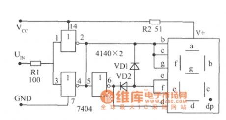
The test circuit diagram composed of 7404 TTL hex not gate is shown as the chart. The TTL (CMOS) circuit hascertain high and low level input threshold voltage, so it does not need additional setup or adjustment, the test results are very accurate. The two non-parallel gates of input side could increase driven capability, high level displays H, low level displays L. As using common anode digital tube, the polarity of VD1, VD2 changes. If it tests CMOS level, you should use a 4069 CMOS NAND gate and so on.
(View)
View full Circuit Diagram | Comments | Reading(1429)
A linear three-terminal regulator expansion flow circuit diagram
Published:2011/6/24 2:16:00 Author:Ecco | Keyword: linear , three-terminal , regulator , expansion flow
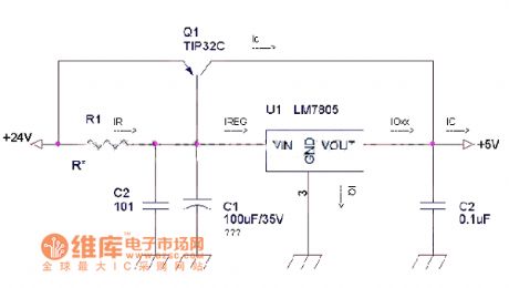
This circuit is an ususal linear three-terminal regulator expansion flow circuit. 1. Drawback of source; 1.1 The power supply is a linear regulator circuit, of which all have their own internal power loss, and voltage drops result in heat loss, and the low efficiency needs us pay special attention on heat issues. 1.2 As the working speed of core component in 7805 is not too high, it has slow response to rapid changes of the input voltage or load current; 1.3 This circuit does not increase the power protection circuit because 7805 itself has overcurrent and temperature protection.
(View)
View full Circuit Diagram | Comments | Reading(666)
CPU fan stopping alarm circuit diagram
Published:2011/6/24 4:17:00 Author:Ecco | Keyword: CPU , fan , stopping alarm
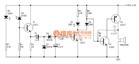
D1 and D2 are respectively the infrared transmitter and infrared receiver tubes, and they are against the installation and 1.2-1.8 cm apart. When it gets power, D1 emits a continuous infrared beam IR, which is intermittently hitting the receiver tube under the block of blade from time to time. This, V1 will have a pulse type of bias current to make the two ends of R2 generate pulse voltage. D4 must use a germanium diode such as 1N60, 2AP9 and so on. SPEAKER can select the type on the quartz clock with pointer.
(View)
View full Circuit Diagram | Comments | Reading(1631)
BCD code LED digital display components frame circuit diagram
Published:2011/5/17 4:18:00 Author:Ecco | Keyword: BCD code, LED , digital , display , components , frame
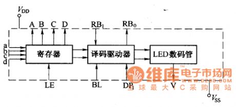
BCD code LED digital display component is a type of display module composed of strong drive CMOS integrated circuit and LED digital display, it has the triple functions of BCD code storaging, decoding drive, LED display.
(View)
View full Circuit Diagram | Comments | Reading(582)
Simple infrared alarm device installation and commissioning circuit diagram
Published:2011/6/24 3:16:00 Author:Ecco | Keyword: Simple , infrared , alarm device, installation , commissioning
The alarm device uses 7812 three-terminal fixed regulator to constitutes a regulated power supply, and it has 14V battery to ensure alarm work reliably and effectively when the AC electric supply power has failure or destroyed case. The infrared light-emitting diode VD1 uses HG504 type, and the operating current is 200mA, and radiation power is 40mW-50mW, then control distance is up to 8 meters, if the control distance is less than 5 meters, it can also use HG410 series. V1 phototransistor can use 3DU31 or 3DU5. The remaining components is chosen according to marked in the figure.
(View)
View full Circuit Diagram | Comments | Reading(549)
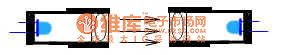
LED +/- symbol display components appearance circuit diagram
Published:2011/5/17 4:17:00 Author:Ecco | Keyword: LED, +/- , symbol, display components, appearance
CL300 Series of LED ± symbol display components have the features of low power consumption, high reliability, long life and other characteristics, they are mainly used in digital instruments, meters and all kinds of digital electronic devices as + , - symbol display. Its shape is shown as the chart.
(View)
View full Circuit Diagram | Comments | Reading(650)
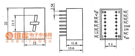
CL328-6-Communication signal chip microcomputer integrated circuit
Published:2011/7/13 4:38:00 Author:leo | Keyword: Signal chip, communication
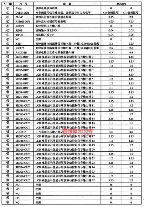
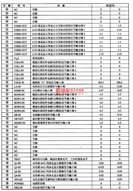
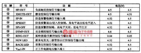
CL328-6 is communication signal chip microcomputer integrated circuit which is widely used in caller ID telephone.1.Function features:CL328-6 contains dual audio signal generator circuit, theft deterrent telephone, pulse signal generator circuit, caller ID decoding circuit, battery under voltage test circuit, ringing test circuit, display drive circuit, key switch RoHS code circuit and others. 2.Pin functions and data:It uses 100-pin soft package and the pin functions as well as related information are shown in the picture 1. (View)
View full Circuit Diagram | Comments | Reading(853)
Electric bridge sensing isolated amplifier circuit diagram
Published:2011/7/1 3:16:00 Author:Rebekka | Keyword: Electric bridge, sensing isolated amplifier
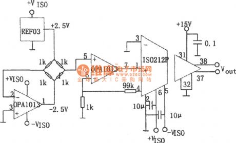
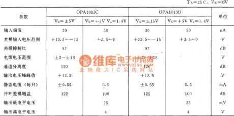
Many sensors, such as the strain gauge platinic resistance, pressure sensor, the gas detection, etc. They use the electric bridge as sampling circuit differential signal. The figure shows the circuit using a single power supply high precision double luck OPA1013 as preamplifier. It uses the double mouth isolation miniaturization isolated amplifier ISO212P as level after isolated amplifier.
(View)
View full Circuit Diagram | Comments | Reading(943)
TRF5O01 GPS RF receiving and collecting integrated circuit
Published:2011/7/13 20:07:00 Author:leo | Keyword: GPS, RF, Integrated circuit
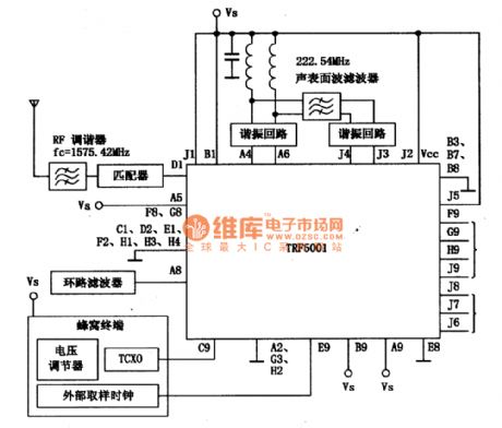
TRF5O01 is a type of GPS RF receiving and collecting integrated circuit used in GPS positioning system.
Function features:
TRF5O01 has the cellular terminal and emitter with sources. It contains low noise amplifier mixer. The first and second LO set-frequency synthesizer and four bit ADC and so on are always used in high sensibility GPS system. TRF5O01 working voltage is 2.7 V to 3.3 Vand the current consumption is super light. When the voltage is 2.7 V, its current consumption is 49 mA. (View)
View full Circuit Diagram | Comments | Reading(988)
LAG665-The single chip stereophonic reproduction integrated circuit
Published:2011/7/13 20:12:00 Author:leo | Keyword: Single chip, Stereophonic reproduction, Integrated circuit
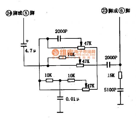
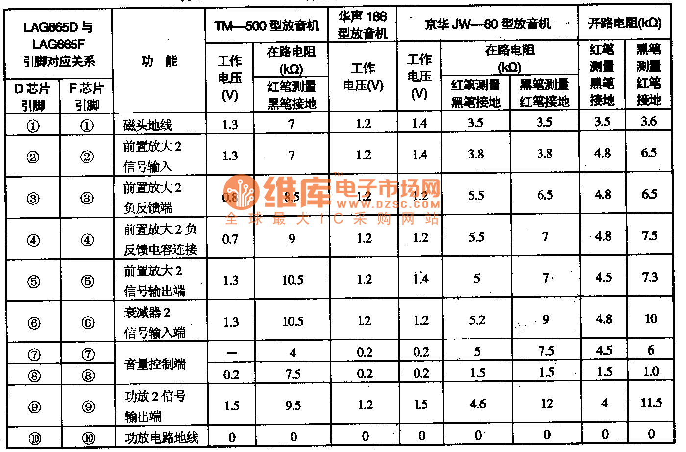
 LAG665 is the third generation single chip personal stereo stereophonic reproduction integrated circuit. It has multiple function and made by MITSVMI.
Inner circuit function:LAG665 has a dual channel front magnetic head amplifier, backward stage earphone drive, double power amplifier and electronic DC volume control function and so on.
Package construction: It has two kinds of package construction. LAG665D adopts 30 pin dual line package. And LAG665F uses 28 pin package construction. They have the same electrical property and inner diagram. (View)
LAG665 is the third generation single chip personal stereo stereophonic reproduction integrated circuit. It has multiple function and made by MITSVMI.
Inner circuit function:LAG665 has a dual channel front magnetic head amplifier, backward stage earphone drive, double power amplifier and electronic DC volume control function and so on.
Package construction: It has two kinds of package construction. LAG665D adopts 30 pin dual line package. And LAG665F uses 28 pin package construction. They have the same electrical property and inner diagram. (View)
View full Circuit Diagram | Comments | Reading(2334)
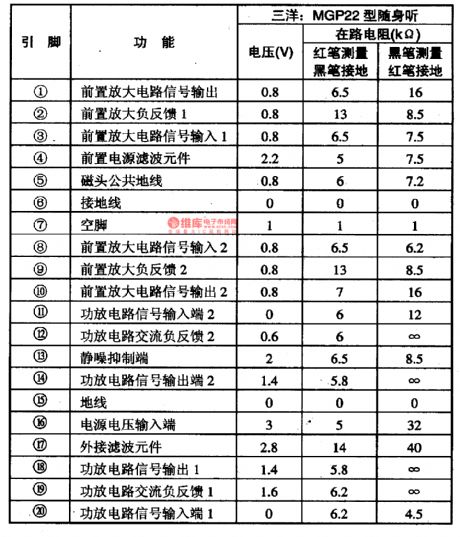
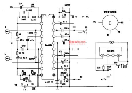
CX20023--the single chip stereo playback integrated circuit
Published:2011/7/12 3:36:00 Author:Borg | Keyword: single chip, stereo, playback, integrated circuit
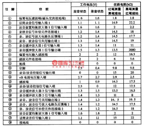
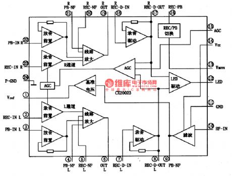
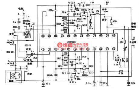
CX20023 is a single chip stereo record/playback integrated circuit, which is often used in walkmen and domestic stereos.1.the internal circuit and pin functions of CX20023CX20023 contains two lines of same microphone recording preamplifier and wire recording amplifier, tape playback balance amplifier, recording LEV auto control and other circuits, whose internal circuit is shown in figure 1. This IC is in the pin in-line plastic structure package, whose pin functions and data are listed in table 1.
(View)
View full Circuit Diagram | Comments | Reading(1164)
The rotate speed test circuit made by optoelectronic transistor
Published:2011/7/13 20:10:00 Author:leo | Keyword: Rotate speed test circuit, Optoelectronic transistor
The picture1 shows rotate speed test circuit made by optoelectronic transistor and so on. When the luminous flux of the optoelectronic transistor VT1 increases by 1%, photo current generates 500 mV voltage between VT2 and VT3. And this voltage is stable logarithm relation under the biggish photoelectic current.Therefore, this circuit can work normally however the optical line changes. A1 and related components form high gain self-adapting filter which can hold down the photo noise in the environment and add clean signals to comparator and input port. (View)
View full Circuit Diagram | Comments | Reading(1032)
Nanjing Iveco A30.10 intermediate/low ceiling light car and Zhongnan air-conditioner system circuit
Published:2011/7/12 7:14:00 Author:Borg | Keyword: Nanjing Iveco, light car, air-conditioner system
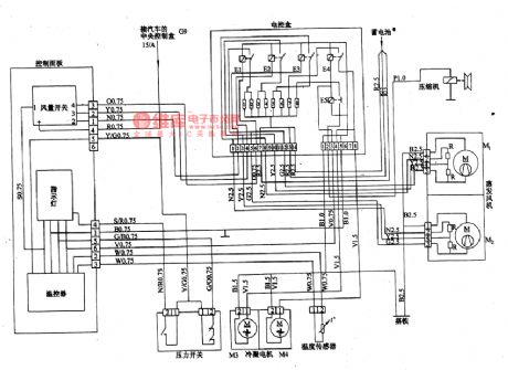
(3)Zhongnan air-conditioner system circuit of Nanjing Iveco A30.10 intermediate/low ceiling light car (see as figure 23) Zhongnan air-conditioner system circuit of Nanjing Iveco A30.10 intermediate/low ceiling light car is shown in figure 23, which has 2 evaporating motors M1 and M2, 2 condensers M3 and M4, there installs a wind switch, a temperature controller and indicator on the control board. The power of the wind switch is from the connection terminal G9 in the central box of the car, which is under the control of the igniting switch. There are 8 fuses in the control box, of which 1 and 2, 3 and 4, 5 and 6 are in parallel connection with each other, but 7 and 8 are not.
(View)
View full Circuit Diagram | Comments | Reading(574)
The timer with definite time opening and closing and automatic circulation function circuit diagram
Published:2011/6/30 1:32:00 Author:Rebekka | Keyword: definite time opening and closing , automatic circulation function
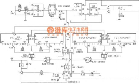
This circuit is a quartz crystal type high precision adjustable timer. It is set by the gears switch time function selection choose and timing. The timing time setting range is 0 ~ 99 s or 0 ~ 99 min. The circuit is shown in figure. The circuit is composed of seconds time, scheduled power circuit, timing boot circuit, regular shutdown circuit, timing cycle control circuit and execution of circuit. (View)
View full Circuit Diagram | Comments | Reading(734)
TOP2l2Y/P/G-PWM single chip switch source integrated circuit
Published:2011/7/13 20:11:00 Author:leo | Keyword: PWM, single chip, integrated circuit
TOP212 is a kind of PWM single chip switch source integrated circuit which is made by Power company in America. It is widely used in DVD, VCD, computer and LCD, air conditioner control system and other home appliances switch power source circuit.
TOP212Y/P/G has three packages which is different from each other from the suffix.(1)TOP212Y. It uses TO-220 package and has small thermal slug. The chip of thermal slug is connected to source S port and belongs to the classical signal line and three ports part.(2)TOP212P. It uses DIP-8 package which belongs to dual line eight pins package. And its pin ①-③ and ⑥-⑧ all connect to source S port. (View)
View full Circuit Diagram | Comments | Reading(560)
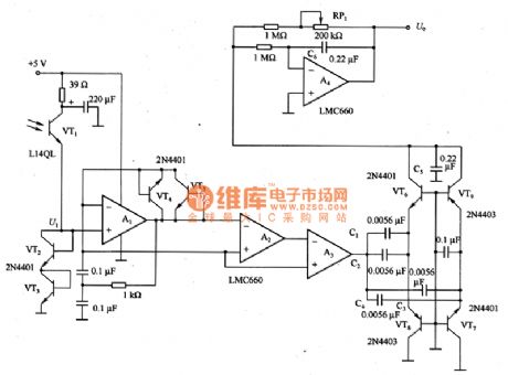
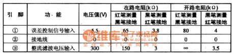
Single-supply inverting amplifier circuit composed of the μA709
Published:2011/6/27 20:15:00 Author:Rebekka | Keyword: Single-supply inverting amplifier
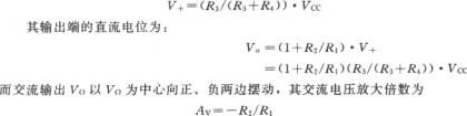
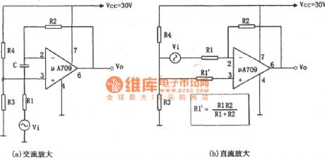
(a),(b)。(a)、(b),R3、R4,:
(View)
View full Circuit Diagram | Comments | Reading(799)
LA4520-Single chip playback integrated circuit
Published:2011/7/13 20:09:00 Author:leo | Keyword: Single chip, playback
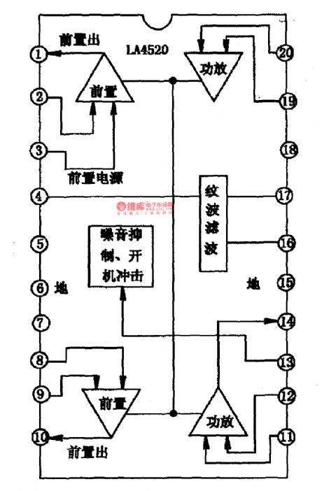
LA4520 is a single chip playback integrated circuit produced by Sanyo Company in Japan, which is widely used in all kinds of playersand recording playback devices. 1. LA4520 inner circuit diagram and pin functions:LA4533M contains two similar fronted power amplifiers, and stereo system circuit. It uses 20-pin dual-line package. The inner circuit diagram of LA4520 is shown in the picture 1-1.2. LA4520 classic applying circuit is shown in the picture 1-2.3. Signal processPicture 1-3 gives the whole process of the play signals. (View)
View full Circuit Diagram | Comments | Reading(1866)
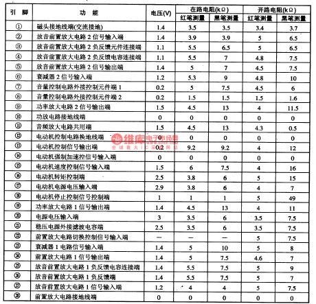
CXA1034P-Single chip stereo integrated circuit
Published:2011/7/13 4:40:00 Author:leo | Keyword: Single chip, stereo
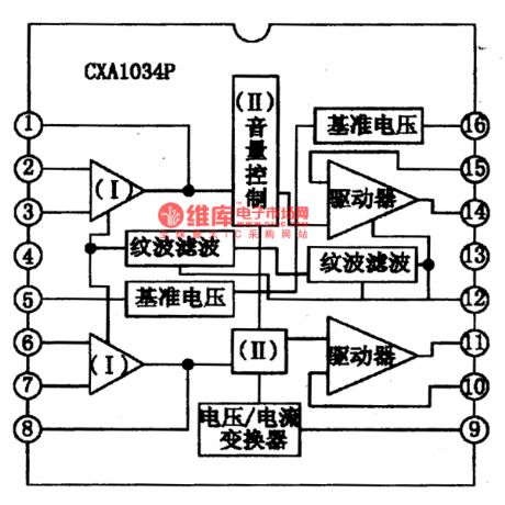
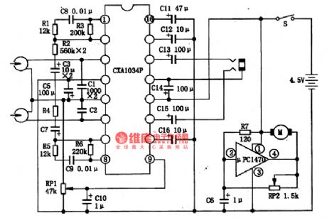
CXA1034P is a single chip playback integrated circuit produced by Sanyo Company in Japan which is widely used in all kinds of low voltage recorders. 1. CXA1034P inner circuit diagram and pin functions:CXA1034P contains two similar fronted power amplifiers, two power amplifiers, less outer components, and single electric voltage controlling stereo volume controller. It uses 16-pin dual-line package. The inner circuit diagram of CXA1034P is shown in the picture 1.2. CXA1034P classic applying circuit is shown in the picture 2.CXA1034P’s power supply voltage is from 1.8 B to 10 V. (View)
View full Circuit Diagram | Comments | Reading(1972)
KA22135-Single chip stereo player integrated circuit
Published:2011/7/13 4:40:00 Author:leo | Keyword: Single chip, stereo player
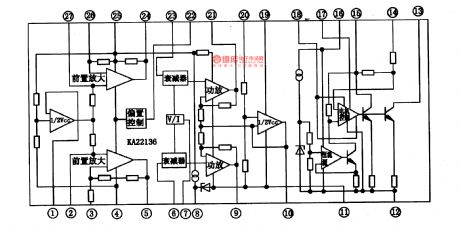
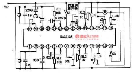
KA22135 is single chip stereo player integrated circuit produced by Samsung in Korea. 1.KA22135 inner circuit diagram and pin functions:KA22135 contains two fronted amplifiers, double power amplifier and electric DC volume control circuit and DC device speed regulator circuit.It has two packages. KA22136F is 28-pin dual line package and KA22136 is 28-pin dual-line flat package. They have the same inner functions and the inner circuit diagram is shown in the picture 1-1.2.KA22135 main parameters:Its work voltage converge is from 2.1 V to 5 V and the classic work voltage is 3 V. When Vcc is 3 V and RL is 32, its output power is 28 mW x 2.3.KA22135 classic applying circuitIts classic applying circuit is shown in the picture 1-2. (View)
View full Circuit Diagram | Comments | Reading(1668)
KA22134-Single chip stereo player integrated circuit
Published:2011/7/13 4:39:00 Author:leo | Keyword: Single chip, stereo player
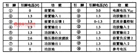
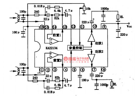
KA22134 is single chip stereo player integrated circuit produced by Samsung in Korea which is used in the low voltage walkman. 1.KA22134 inner circuit diagram and pin functions:KA2214 contains two fronted amplifiers, double power amplifier and electric DC volume control circuit and DC device speed regulator circuit.It uses 16-pin dual line package and the inner circuit diagram is shown in the picture 1-1.2.KA22134 main parameters:Its work voltage converge is from 1.8 V to 6 V and the classic work voltage is 3 V. (1)Maximum output voltage of fronted amplifier Vom. When THDI is 10%, its value is 770mV. (2)The output power of driver Po. When THD2 is 10%, its classic value is 30 dB. (View)
View full Circuit Diagram | Comments | Reading(1983)
| Pages:1541/2234 At 2015411542154315441545154615471548154915501551155215531554155515561557155815591560Under 20 |
Circuit Categories
power supply circuit
Amplifier Circuit
Basic Circuit
LED and Light Circuit
Sensor Circuit
Signal Processing
Electrical Equipment Circuit
Control Circuit
Remote Control Circuit
A/D-D/A Converter Circuit
Audio Circuit
Measuring and Test Circuit
Communication Circuit
Computer-Related Circuit
555 Circuit
Automotive Circuit
Repairing Circuit