
Circuit Diagram
Index 1540
Op amp instrumentation circuit diagram
Published:2011/6/24 2:36:00 Author:Ecco | Keyword: Op amp , instrumentation
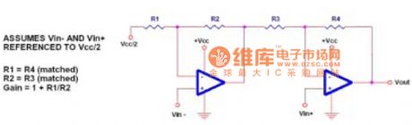
In many cases, the op amp input end is connected to the capacitor to prevent DC level caused by virtual ground. This capacitor is actually a high-pass filter, in a sense, all single-supply op amp circuits like this have such a capacitor. Filter implementation is simple, but the designer must pay attention to the following points: 1. Filter inflection point (center) frequency; 2. the gain of the filter circuit; 3. Q value of of bandpass filter and band stop filter; 4. low-pass and high-pass filter types (Butterworth, Chebyshev, Bessell).
(View)
View full Circuit Diagram | Comments | Reading(563)
FET DC power amplifying circuit
Published:2011/7/13 20:04:00 Author:leo | Keyword: FET, DC power amplifying, Circuit
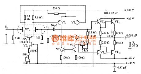
Picture 1 shows a FET DC power amplifying circuit. VT1 is the difference amplifying circuit, while VT2 is the constant current differential circuit. And VT5 is electrical level moving circuit made by cascading amplifiers. The source voltage of VT3 is about 0.6 V and VT7 and VT8 are current mirror circuit which is used to aggrandize gain and improve the DC operating point stability. VT6 is the circuit that offers differential current to output terminal.
(View)
View full Circuit Diagram | Comments | Reading(974)
A FET audio amplifying circuit
Published:2011/7/13 20:05:00 Author:leo | Keyword: FET, Audio, Amplifying circuit
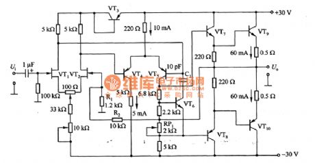
Picture 1 shows a FET audio amplifying circuit which demands small distortion, broad frequency bandwidth. The input terminal uses Knot type FET which can eliminate the influence to circuit caused by change of source voltage and current moving. DC stability is the main problem of direct-coupling DC amplifier which needs to use two level difference circuits. The first level difference circuit is formed by N channel FET, VT1 and VT2. The second level difference circuit is formed by PNP, VT4 and VT5, which has a high voltage amplitude of vibration and bigger distortion that should be paid attention during design. (View)
View full Circuit Diagram | Comments | Reading(1092)
Maintenance circuit diagram of microprocessor partial failure
Published:2011/6/24 2:58:00 Author:Ecco | Keyword: Maintenance circuit , microprocessor, partial failure
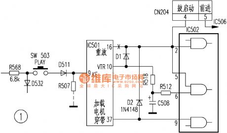
Figure 1 is a schematic diagram of the machine, when you press the playback button PLAY (SW503), pin {18} the address signal of IC501 (μPD7538C) is the high start pulse signal by sent to pin 9 after passing the R568, SW503, D511. The internal circuit of microprocessor will generate IC501 playback control commands, so that pin {16} high will output 4 9V high level, of which one way is sent to the pin 4 of CN204 to drive the drum motor, and another way is sent to pin 2 and pin 5 of IC502. The dominant axis motor of IC501 is positive rolling , the pin {34} of control commands output end is also in high level, which is added to pin 5 of CN204 by IC506 to drive the capstan motor be positive rolling.
(View)
View full Circuit Diagram | Comments | Reading(730)
Touch-switch desk lamp circuit diagram
Published:2011/5/13 4:26:00 Author:Ecco | Keyword: Touch-switch, desk lamp
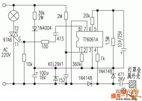
Touch-switch desk lamp circuitry is as below: It's divided into four gearsto control lamps. When it gets power and the lamp is not lit, touching the metal surface of lampshade firstly will emit the light in low brightness; touching the lamp secondly will emit proper light; touching the lamp thirdly will turn on the light absolutely, and touching the lamp fourthly will turn off the light, and the order is just like this. In the circuitry, TT6061 could be replaced by GS6061, IN4004 could be replaced by IN4007.
(View)
View full Circuit Diagram | Comments | Reading(4032)
The circuit diagram composed of ZHF-9901 and ZHJ-9902
Published:2011/5/13 4:28:00 Author:Ecco
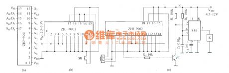
Integrated IR remote control module is a high integrated, fully functional infrared remote control transmitter module. ZHF-9901/03/05 is the transmitting module, ZHJ-9902/04/06 is the receiving module. (b) is a single touch-tone single infrared remote control launcher. (c) is an infrared receiving circuit composed of ZHJ-9902. (View)
View full Circuit Diagram | Comments | Reading(782)
NEC N—831 VCR common breakdown maintenance circuit diagram
Published:2011/6/24 3:50:00 Author:Ecco | Keyword: NEC , VCR, common breakdown , maintenance
When the power switch is turned on, the electronic viewfinder image is normal, pressing the power zoom key T (Telephoto), when the scene is near the target, the inside viewfinder image is blurred. Analysis and Maintenance: When shooting, pressing the T key and when the scene is near the target and the viewfinder image is blurred, it should be noticed that the focus ring does not rotate, then you should check the camera focus selecting switch on the control panel (FOCUS) has been pulled to AUTO position; rotateing the focus ring to observe the clarity of the viewfinder image is back to normal level or not,then you can determine the failure's existence being in auto-focus detection control and motor drive circuit.
(View)
View full Circuit Diagram | Comments | Reading(1331)
Multichannel infrared remote control circuit diagram composed of LM567
Published:2011/5/13 4:28:00 Author:Ecco | Keyword: Multichannel , infrared remote control
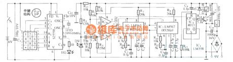
LM567 is a PLL audio decoding circuit
(View)
View full Circuit Diagram | Comments | Reading(1382)
The automatic door control circuit diagram with infrared sensor IC WT8075
Published:2011/5/13 4:29:00 Author:Ecco | Keyword: automatic door, control circuit , infrared sensor, IC

The circuitry is shown as below: It includes pyroelectric infrared sensor head, infrared sensor control circuit, SCR control circuit, music sound circuit and exchange step-down rectifier circuit, etc. (View)
View full Circuit Diagram | Comments | Reading(3403)
Infrared sensing automatic startup control circuit diagram with SR5553
Published:2011/5/13 4:29:00 Author:Ecco | Keyword: Infrared sensing automatic startup control
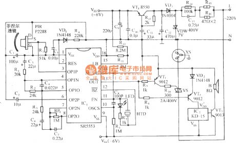
The circuitry shows as below: It includes pyroelectric infrared sensor head, infrared sensor control circuit, SCR control circuit, music sound circuit and exchange step-down rectifier circuit, etc. This control circuit can be used as control of automatic fan boot, automatic, energy-saving lamps, security, automatic interpretation etc. Pyroelectric infrared sensor head includes pyroelectric infrared sensor P2288 and the Fresnel optical lenses. The latter connects the infrared radiation that is from human body energy, to improve the detection range. The Fresnel lens have all sorts of different specifications, common have Q - 6 type, Q1A type and Q - 8 type, etc. To make energy‘s largest gathered, it requests lens face and infrared sensors to keep a certain distance, to different lens, their spotlighting distance is different. The reasonable configuration and installing can make detection distance be improved greatly. P2288 will detect the infrared radiation that from the pedestrians, then make impedance matching and magnifiing by the filter, signal mosfet (FET), emitted by source S to the signal input (IC1 OP1P) pin 3. (View)
View full Circuit Diagram | Comments | Reading(1686)
Panasonic NV-L15 VCR breakdown maintenance circuit diagram
Published:2011/6/24 3:59:00 Author:Ecco | Keyword: Panasonic , VCR , breakdown maintenance
Fault phenomenon: When it is connected to the power, the display has a clock display. Pressing the power switch and turning on the power, but the cassette tape can not be pullin into storage box. Analysis and Maintenance: The chart shows the connection circuit with box. Under normal circumstances, when the cartridge is pulled into the cassette, the mechanical transmission mechanism of storage with box will drive the switch with box which is intalled on the right side of plastic bracket in mechanism components with storage box. The switch with box has three different sliding contact positions of A, B, C , which are used to monitor the tape location in the box and notify the microprocessor (CPU) to issue the appropriate instructions.
(View)
View full Circuit Diagram | Comments | Reading(1571)
Household AC voltage regulator principle and maintenance circuit diagram
Published:2011/6/24 4:05:00 Author:Ecco | Keyword: Household, AC voltage regulator, principle , maintenance
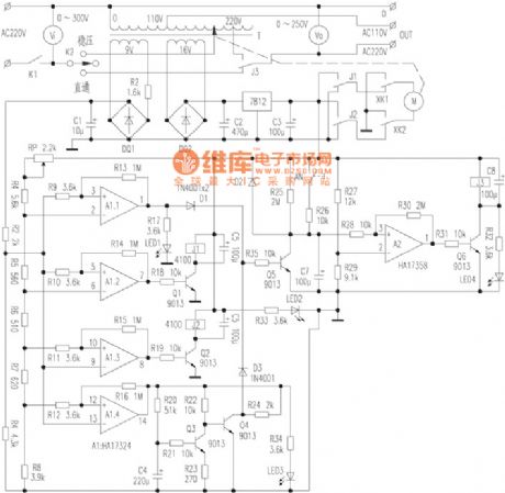
The Dadi TJ30 3kW AC voltage regulator electrical schematic is shown as the chart. The whole machine can be divided into two parts of the main circuit and control circuit, and Vi and Vo are the input and output tables. The main circuit is the path of the AC power from input end to output end, and the path includs air switch K1, regulator and direct connection selecting switch K2, regulator transformer T, delay control relay J3 and input and output wiring terminals and other components. Control circuit has the functions of power delay transmission, stable output voltage, overvoltage protection and instructions, undervoltage protection and indication.
(View)
View full Circuit Diagram | Comments | Reading(1553)
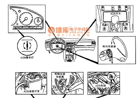
Benz W129 (KE System Engine) ADS system, component location circuit diagram
Published:2011/6/23 2:41:00 Author:Ecco | Keyword: Benz , KE System Engine, ADS system, component location
View full Circuit Diagram | Comments | Reading(503)
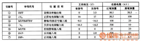
TDA7496 two-channel audio power amplifier integrated circuit diagram
Published:2011/5/17 4:10:00 Author:Ecco | Keyword: two-channel , audio , power amplifier , integrated circuit
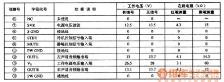
TDA7496 is the two-channel audio power amplifier IC produced by Philips, it is widely used in the high-fidelity audio, car audio, multimedia and so on. 1. Features of functionTDA7496 integrated circuit contains two audio power amplifier circuits with the same functions, and it has electronic volume control circuit, the squelch control circuit, overheat protection and short circuit protection, mono output power is 6W, limit working voltage is 30V. 2. Pin functions and data TDA7496 IC uses 15-pin single in-line package, the pin functions and data are listed in Table 1. Table 1 shows TDA7496 integrated circuit pin functions and data.
(View)
View full Circuit Diagram | Comments | Reading(1572)
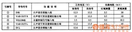
TDA7495 two-track audio power amplifier integrated circuit diagram
Published:2011/5/17 4:10:00 Author:Ecco | Keyword: two-track , audio, power amplifier, integrated circuit
TDA7495 is the two-channel audio power amplifier integrated circuit produced by Philips, it is widely used in home hi-fi, television, stereo, car audio and multimedia audio. 1. The featuresand functionsTDA7495 integrated circuit contains two audio power amplifier circuits with the same features, and it also has two independent mute function with thermal overload protection and short circuit protection, and output power is 20W. 2. Pin functions and data TDA7495 IC uses 15-pin single in-line package, the pin functions and data are listed in Table 1. Table 1 shows TDA7495 integrated circuit pin functions and data.
(View)
View full Circuit Diagram | Comments | Reading(977)
The saving lamp circuit diagram and maintenance
Published:2011/6/24 3:06:00 Author:Ecco | Keyword: saving lamp , maintenance
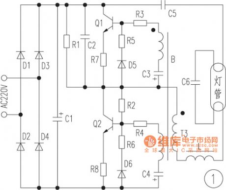
The saving lamp circuit has the glass cover type and exposed type. Glass cover types have three series of spherical, cylindrical ball, processing type, etc. , the first two series have completely four types of transparent, carving, engraving and white color. It has the advantages of beautiful appearance, easy installation, anti-collision, etc.; exposed type has the types of H, UH-based, 3U, 4U-based, 2D and screw type. They also can be divided by the color of light, which can be divided into red, green, blue, yellow (color temperature is 2700K, and it belons to warm light which is similar to incandescent light color), white (color temperature is 6400K, is a cool light which similar to fluorescent light color); the lamps with color temperature in 5000K has no irritation to the eyes as the light color close to natural light.
(View)
View full Circuit Diagram | Comments | Reading(664)
TDA7298 high-fidelity AB audio power amplifier IC diagram
Published:2011/5/17 4:10:00 Author:Ecco | Keyword: high-fidelity , AB , audio power, amplifier, IC
TDA7298 is high-fidelity AB audio power amplifier IC produced by SGS in Europe, it is widely used in high-Rover, TCL, and other large-screen color TV. 1.The featuresand functionsTDA7298 integrated circuit is primarily composed of power amplifier, mute / standby control circuit, over current and short circuit protection circuit. When Vcc = ± 22V, RL = 4Ω, RL = 8Ω, the output power can reach 28W. 2. Pin functions and data TDA7298 IC uses the package with 7 pin in single row, the pin functions and data are listed in Table 1.Table 1 shows TDA7298 integrated circuit pin functions and data
(View)
View full Circuit Diagram | Comments | Reading(1302)
3 different ways of driving high-power control circuit diagram
Published:2011/5/17 4:11:00 Author:Ecco | Keyword: 3 , different ways , driving , high-power, control circuit
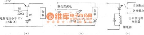
The figure shows the 3 different ways of driving high-power control circuit. Flashing light-emitting diodes can be used as high-power multi-center load control circuit devices to drive a variety of incandescent light flashes. Figure (a) uses high-power transistor to drive circuit; Figure (b) uses high-power bidirectional thyristor to controll driver circuit; Figure (C) uses relay to control the load. VT can choose 3AD, 3CD PNP power transistor. SCR can also use one-way, but the load current is pulsating DC current. The load of the 3 circuits flashes intermittently under the control of light-emitting diode.
(View)
View full Circuit Diagram | Comments | Reading(539)
The auto reverse anti-collision ultrasonic radar circuit diagram
Published:2011/6/24 4:10:00 Author:Ecco | Keyword: auto reverse , anti-collision, ultrasonic radar
The ultrasonic radar circuit's design is reasonable,and it has been several field trials,and it works reliably. The circuit is sealed by the ultrasonic sensor R/S40 (including transmit and receive), the signal receiving and processing control circuit, alarm, display circuit and power supply etc., and the circuit is shown in photo. Each part of the circuit is described below. The ultrasonic sensor R/S40 in the circuit is not only used for transmitting ultrasound, but also receiving the reflected echo, so it has a two-way transmit / receive function.
(View)
View full Circuit Diagram | Comments | Reading(3411)
LED power supply voltage multiplier circuit diagram
Published:2011/5/17 4:11:00 Author:Ecco | Keyword: LED, power supply, voltage multiplier
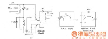
The power supply voltage multiplier conversion circuit is shown as the chart. In electronic circuit design, some amplifiers require low current and high voltage, they can use flashing LED and few components to make a DC voltage multiplier conversion circuit. In the Figure (a), it uses capacitors C1, C2 to store charge, the flashing LED's own oscillations can drive relay switch conversion, and the supply voltage and C1 are continuously superimposed, and it will get a twice supply voltage on C2, the output current is about 10mA. Relay uses 6V or 30mA, Figure (b) is the multiplier principle diagram.
(View)
View full Circuit Diagram | Comments | Reading(839)
| Pages:1540/2234 At 2015211522152315241525152615271528152915301531153215331534153515361537153815391540Under 20 |
Circuit Categories
power supply circuit
Amplifier Circuit
Basic Circuit
LED and Light Circuit
Sensor Circuit
Signal Processing
Electrical Equipment Circuit
Control Circuit
Remote Control Circuit
A/D-D/A Converter Circuit
Audio Circuit
Measuring and Test Circuit
Communication Circuit
Computer-Related Circuit
555 Circuit
Automotive Circuit
Repairing Circuit