
Circuit Diagram
Index 1527
Nickel cadmium battery automatic charging and discharging device
Published:2011/7/14 20:37:00 Author:TaoXi | Keyword: Nickel cadmium battery, automatic, charging, discharging, device

Charging process: if you set the switch S to position 1 , and put the batteries into the battery clip, then connect the power, the pin-2 of TL082 has the voltage of 3V, but the pin-3 voltage is lower than 3V, the pin-1 outputs the negative voltage, BG cuts off, J has no current, the normally closed contact point J1 closes, the power charges the battery through the R8, S2, J1. When the battery voltage is higher than 3V, the output voltage of pin-1 is positive to conduct the BG, J gets power to cut off J1, the charging completes. At this time the pin-3 of TL082 has the higher voltage which is supplied by R8 and S2 to maintain J's conduction until the power is cut off.
(View)
View full Circuit Diagram | Comments | Reading(851)
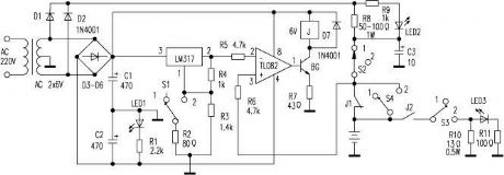
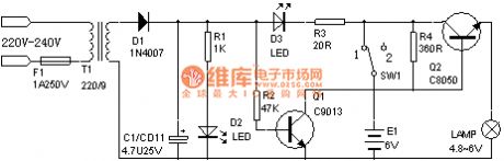
Automatic power off charger circuit
Published:2011/7/14 20:53:00 Author:TaoXi | Keyword: Automatic, power off, charger circuit
Operating principle:
The circuit is as shown in figure 4-31, the whole circuit is composed of rectifier and filter circuit, the constant current charging circuit, the timing control circuit, because the timer's accuracy requirement is not high, so we can use the simple rectification circuit. The charging part uses the constant current charging mode, the circuit is simple and the effect is good. The timing part uses the composite tube operating mode.
When you press S, the 220V AC current is reduced, rectified and filted by the T, VD1-VD4 and C1, so we get the 12V DC. The 12V DC not only supplies the charging voltage to the VD5, R1 and LED, but also charges C2 through S2.
(View)
View full Circuit Diagram | Comments | Reading(789)
Motorola 168VA cell phone car charger
Published:2011/7/14 21:04:00 Author:TaoXi | Keyword: Motorola, cell phone, car, charger

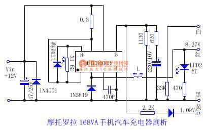
There is one kind of car charger that is suitable for the Motorola 168VA cell phone, it's volume is small and exquisite, and it can directly plug into the car cigarette lighter socket. But it has no circuit diagram, so the maintenance is inconvenience. The measured circuit is as shown in the figure for reference.
The UTC34063 is the 8-pin dual-row DIP IC, it is the single chip buck-boost DC converter control IC. This IC has the temperature compensator, the comparator, the high current output switch. The oscillation frequency is 100KHz. The measured data is as shown in the table.
Pin .....Resistance ......Voltage(V)......Red measurement(KΩ) Black measurement(KΩ) 1 ......4.1 ......8.2 .......12 2 ......0.8...... 7.8...... 8.28 3 ......5.8 ......22 .......0.65 4 .......0 ........0......... 0 5 .......1........ 1 .......1.26 6 ......4.2 ......8.2 .......12 7 ......4.2 ......8.2 .......12 8 .......5........ 10 ......10.6
(View)
View full Circuit Diagram | Comments | Reading(2211)
Pulse type automatic charger circuit (3)
Published:2011/7/14 21:17:00 Author:TaoXi | Keyword: Pulse type, automatic, charger circuit
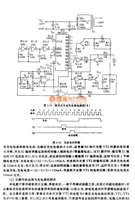
Operating principle:
The circuit principle diagram of this charger is as shown in figure 4-13. The power transformer T1 changes the 220V AC into the 9V AC, and this 9V AC is rectified by VD1 and VD2, then it is filted by C3 to supply the 12V DC voltage to the charger, the capacitance C4 can be used in filtering. The oscillator is composed of the IC1:A, IC2:B and the external components, IC1:C is the buffer stage of the oscillator, the output of IC1:C supplies the clock pulse for the counter IC2. IC2 is the decimal counter, it can be used to control the charging time and discharging time of the charger, and it counts the lower edge of the clock pulse. The charging and discharging timing sequence is as shown in figure 4-14.
(View)
View full Circuit Diagram | Comments | Reading(737)
Pulse type automatic charger circuit (2)
Published:2011/7/14 21:29:00 Author:TaoXi | Keyword: Pulse type, automati, charger
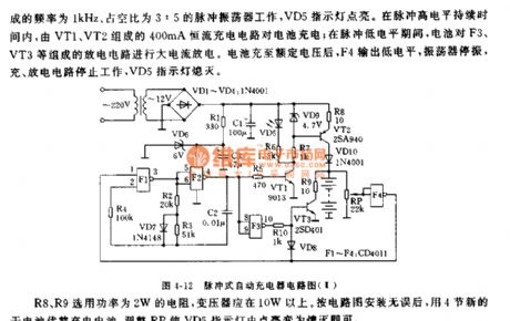
The pulse type automatic charger that is composed of the single chip manifold block CD4011 and a few external components, it can supply the large current pulse type charging and discharging for four Nickel cadmium batteries with the charge-discharge ratio of 7:2, and when the battery is full, it will stop charging automaticly. The features of this circit is simple and practical.
As the figure 4-12 shows, when the circuit is operating, the input port F4 has the low level, the high level of the inverted output controls the pulse oscillator with the frequency of 1 kHz and duly ratio of 3:5. The VD5 indicator lamp turns on.
(View)
View full Circuit Diagram | Comments | Reading(730)
Pulse type automatic charger (1)
Published:2011/7/14 21:53:00 Author:TaoXi | Keyword: Pulse type, automatic charger
Operating principle:
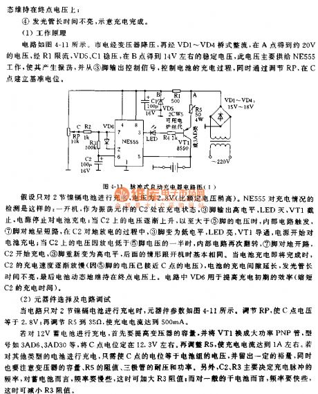
The circuit is as shown in figure 4-11, the city electricity is reduced by the transformer and is bridge-type rectified by VD1-VD4, so point A gets the 20V voltage, this voltage is limited by R1, stabilized by VD5 and C1, so point B gets the 14V stabe voltage, this voltage is supplied to NE555, so the NE555 produces the oscillation and outputs the control signal from pin-3 to control the charging process, by adjusting RP, we can establish the reference potential at C point.
IF you want to charge the 12V storage battery, you need to improve the transformer capacity, and the VT1 need to use the high power PNP transistor such as the 3AD6, 3AD30. The electric potential of point C is about 12.3V.
(View)
View full Circuit Diagram | Comments | Reading(698)
Lithium ion battery charger circuit (3)
Published:2011/7/14 22:36:00 Author:TaoXi | Keyword: Lithium ion battery, charger
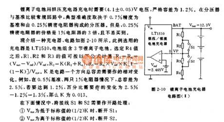
When the lithium ion battery is charging with the constant voltage charger, you need to use the 4.1+/-0.05V voltage, the strict tolerance is 1.2%. In the voltage divider and the benchmark comparison conventional circuit, the typical accuracy depends on the voltage divider which is composed of the electrical resistor with the 0.7% accuracy and 0.25% precision. The price of the 0.25% precision resistor is three times of the 1% precision resistor, and it is hard to find.
Here we introduce one kind of charger, the circuit is as shown in figure 2-10. The charger is LT1510, the battery pack has three Lithium ion batteries. If you choose the value of R4, the values of R1,R2,R3 can be calculated by the formula.
(View)
View full Circuit Diagram | Comments | Reading(813)
Lithium ion battery charger circuit (2)
Published:2011/7/14 23:02:00 Author:TaoXi | Keyword: Lithium ion battery, charger circuit
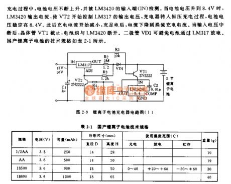
The simplest Lithium ion battery charger circuit is as shown in figure 2-9. This charger uses the lithium ion battery charging controller LM3420-8.4, it can charge two series lithium-ion battery groups. When the voltage of the battery group is lower than 8.4V, the output port of LM3420 has no output current, the transistor VT2 cuts off, so the adjustable voltage-regulator tube LM317 outputs the constant current. The rated output current of the LM317 is 1.5A, if you need the larger charging current, you can use LM350 or LM338.
In the charging process, the battery voltage rises and it is detected by the output port of LM3420. When the battery voltage is 8.4V, the LM3420 outputs the current to make the VT2 control the output voltage of LM317.
(View)
View full Circuit Diagram | Comments | Reading(2638)
Concise parallel automatic charger circuit
Published:2011/7/15 0:41:00 Author:TaoXi | Keyword: Concise, parallel, automatic, charger
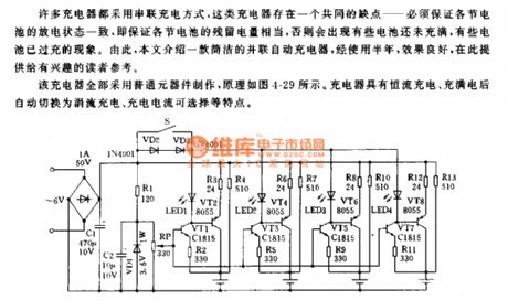
A lot of chargers use the series charging mode, these chargers have a common shortcoming--you need to guarantee that every battery has the same residual power, otherwise some batteries are overcharging but some batteries are insufficient charging. So this artical introduces one kind of concise parallel automatic charger which has good effect.
This charger is composed of the common components, the principle is as shown in figure 4-29. The charger has the features of constant current charging, automatic switchover (trickle charge), and the optional charging current.
(View)
View full Circuit Diagram | Comments | Reading(753)
Rechargeable flashlight circuit one (4)
Published:2011/7/15 0:44:00 Author:TaoXi | Keyword: Rechargeable, flashlight
View full Circuit Diagram | Comments | Reading(1553)
Digital Temperature Meter Circuit
Published:2011/7/17 8:23:00 Author:Robert | Keyword: Digital, Temperature, Meter
The picture shows the digital temperature meter circuit. (View)
View full Circuit Diagram | Comments | Reading(1518)
Class B Amplification Complementary Symmetry Working Principle Circuit
Published:2011/7/15 19:51:00 Author:Robert | Keyword: Class B, Amplification, Complementary, Symmetry, Working, Principle
The picture shows the class B amplification complementary symmetry working principle circuit.
(1)Its working principle.
Static: IB=0, IC=0, uo=0
Dynamic:
When it is in the ui's positive half cycle, the NPN transistor is in the mode of amplification and the PNP transistor is cloced. The current through RL is iC1.
When it is in the ui's negative half cycle, the PNP transistor is in the mode of amplification and the NPN transistor is cloced. The current through RL is iC2. (View)
View full Circuit Diagram | Comments | Reading(746)
Buick GL8 Car TPM Circuit
Published:2011/7/15 20:11:00 Author:Robert | Keyword: Buick, GL8, TPM
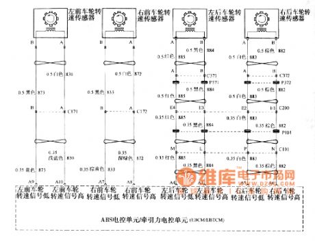
The picture shows the Buick GL8 car TPM circuit.
The circuit shows the ABS electronic control unit and the traction electronic control unit. (View)
View full Circuit Diagram | Comments | Reading(456)
TDA2003 Power Amplifier Circuit
Published:2011/7/15 20:13:00 Author:Robert | Keyword: Power, Amplifier
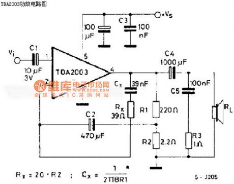
The picture shows the TDA2003 power amplifier circuit. (View)
View full Circuit Diagram | Comments | Reading(1175)
LM1876 Power Amplifier Circuit
Published:2011/7/15 20:23:00 Author:Robert | Keyword: Power, Amplifier
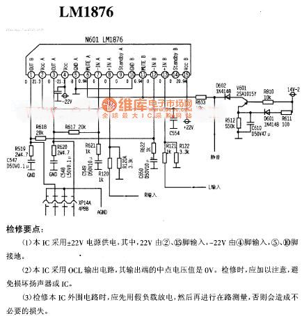
The picture shows the LM1876 power amplifier circuit.
Maintenance points:
(1)This IC uses +/-22V power supply. The 22V should input to pin 2 and pin 15 and the -22V should input to pin 4. The pic 5 and pin 10 should be connected to the ground.
(2)This IC uses OCL output circuit and the output port's middle point's voltage is 0V. When this circuit needs maintenance it should be noticed to avoid to damage the speaker or IC.
(3)When the IC's external circuit needs maintenance it should use a dummy load for discharging and then do the measurement on the circuit. Otherwise it may cause unnecessary damage. (View)
View full Circuit Diagram | Comments | Reading(6327)
LM317 Current-Expansion Circuit (2)
Published:2011/7/16 6:29:00 Author:Robert | Keyword: Current, Expansion
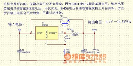
The picture shows the LM317 current-expansion circuit (2).
This circuit is also OK. But its output voltage may be unstable. Because the LM317's pin 1-2 is the reference voltage and the output voltage would minus the power transistor's B-E junction voltage. Not only this, the B-E junction voltage also would decrease while the transistor's temperature increasing. So the output voltage mey be unstable and it's not recommended to do this. (View)
View full Circuit Diagram | Comments | Reading(5087)
LM317 Current-Expansion Circuit (1)
Published:2011/7/16 7:42:00 Author:Robert | Keyword: Current, Expansion
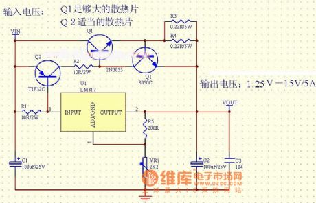
The picture shows the LM317 current-expansion circuit (1).
The input voltage is VIN.
The Q1 needs a large-enough heatsink.
The Q2 needs a adequate heatsink.
The output voltage is 1.25V-15V/5A. (View)
View full Circuit Diagram | Comments | Reading(3283)
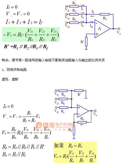
In-Phase Summation Circuit
Published:2011/7/16 6:46:00 Author:Robert | Keyword: In-Phase, Summation
1.This is the in-phase summation circuit.
With the concepts of virtual short circuit and virtual open circuit, we get the single operational amplifier summation-difference circuit anddual operational amplifier summation-difference circuit. (View)
View full Circuit Diagram | Comments | Reading(925)
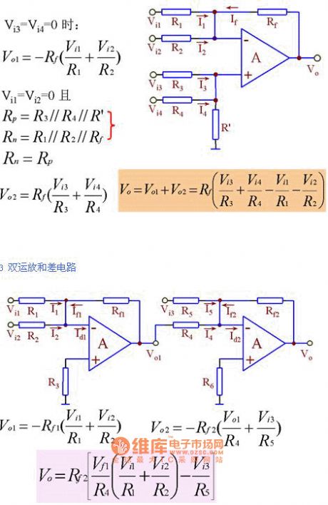
Addition And Subtraction Operation Circuit
Published:2011/7/16 6:53:00 Author:Robert | Keyword: Addition, Subtraction, Operation
1.Out-phase summation circuit.
Virtual short circuit and virtual open circuit.
Feature:if adjusting one channel signal's input resistance it would not affect other channel's input and output ratio.
2.In-phase summation circuit.
Virtual short circuit and Virtual open circuit. (View)
View full Circuit Diagram | Comments | Reading(598)
LM4915 Used In Double-Channel Amplification Circuit
Published:2011/7/16 8:09:00 Author:Robert | Keyword: Double-Channel, Amplification
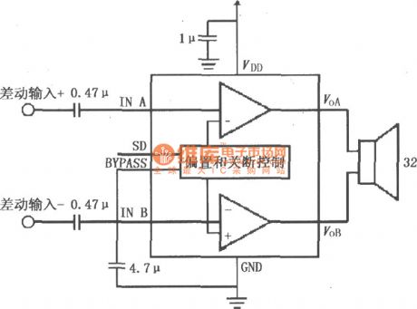
The picture shows the LM4915 used in double-channel amplification circuit. The left, right sound-channel signals would input to the LM4915's pin 8 and pin 3 separately. After the internal amplifier's amplification the signals would output from the pin 6 and pin 5 separately and then coupling on their own sound-channel speaker directly. The LM4915 amplifier gain is determined by its internal resistance Ri and Rf and the internal certain gain is set to 6dB. The amplifier's maximum power consumption would be PDMAX=4VDD2/π2RL in push-pull output coupling mode and would be PDMAX=VDD2/π2RL in single-port output coupling mode. fc=1/2πRiCi and the Ri=20kΩ. The LM4915's pin 1 is connected external closing control switch. When the pin 1 is connected to high voltage level, (1.8V could be high voltage level), it would allow to work. When the pin 1 is connected to low voltage level, (0.4V could be low voltage level), it would prohibit working to reduce the chip's power consumption. (View)
View full Circuit Diagram | Comments | Reading(602)
| Pages:1527/2234 At 2015211522152315241525152615271528152915301531153215331534153515361537153815391540Under 20 |
Circuit Categories
power supply circuit
Amplifier Circuit
Basic Circuit
LED and Light Circuit
Sensor Circuit
Signal Processing
Electrical Equipment Circuit
Control Circuit
Remote Control Circuit
A/D-D/A Converter Circuit
Audio Circuit
Measuring and Test Circuit
Communication Circuit
Computer-Related Circuit
555 Circuit
Automotive Circuit
Repairing Circuit