
Circuit Diagram
Index 1537
Loop elimination, cold junction compensation and high-end thermocouple amplifier circuit diagram
Published:2011/6/23 2:41:00 Author:Ecco | Keyword: Loop elimination, cold junction compensation , high-end , thermocouple amplifier
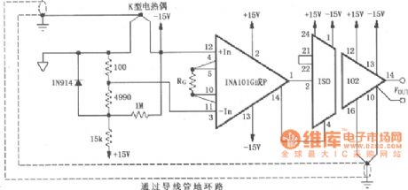
The loop elimination, cold junction compensation and high-end thermocouple amplifier circuit composed of ISO102 and INA101are shown as the chart, it has the fuctions of ground loop elimination, cold junction compensation and high-end off. This circuit uses the K thermocouple to test temperature in the field, the temperature signal is converted to voltage signal, amplified by instrumentation amplifier INA101 and sent to ISO102, isolated and amplified, output by ISO102. Resistor Rc is used to set the INA101's gain. The feature of circuit is that K thermocouple is connected to the ground of ISO102 secondary side, then it will form the same potential, thereby it eliminates the interference caused by ground loop.
(View)
View full Circuit Diagram | Comments | Reading(1926)
555 IC automatic battery charger circuit diagram(2)
Published:2011/5/11 4:06:00 Author:Ecco | Keyword: 555, IC , automatic , battery charger
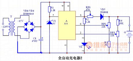
RS flip-flop is composed of A 555 circuit, The two internal comparator reference voltage is supplied by external regulator VS commected to pin 5, so the reset level of circuit is VS's regulator value, which is 3V. The seting circuit of the upper limit charge voltage is composed of the resistor R3 and potentiometer RP2; The seting circuit of the lower limit charge voltage is composed of potentiometer RP3 and resistor R4. The power supply is stepped-down by the T transformer, rectified by diodes VD1 ~ VD4 and filtered by capacitors C1.VD1 ~ VD5 use IN4001 rectifier diodes. VS selects 3V, 1/2W Zener diode, such as UZ-3.0B, IN5226. VL uses an ordinary red LED. RP selects 2W wirewound potentiometer; RP2, RP3 use an ordinary small-scale synthesis of carbon potentiometer, such as WH5; R1 ~ R4 select 1/8W carbon film resistors. C1 selects CD11-25V aluminum electrolytic capacitor. T uses 220V/15V, 5VA small, high quality power transformer.
(View)
View full Circuit Diagram | Comments | Reading(7377)
The 1.25~27V adjustable power supply circuit diagram composed of μA723 high definition IC
Published:2011/5/11 4:14:00 Author:Ecco | Keyword: 1.25~27V , adjustable , power supply, high definition , IC
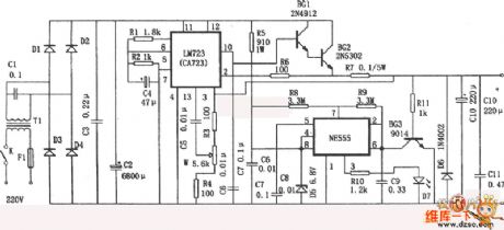
This power supply circuitis composed ofthe high definition integrated circuit μ A723 . The characteristics are as below: (1)The output voltage is adjustablein the range of 1.25~27 V. (2)Having current limiting safeguard function. While output current ≥ 6.5 A , the internal current limitingcircuit of μ A723turns onto protect voltage regulator. (3)The voltage stabilizes well, the currentis inthe range of0~4.5 A, output voltage changes 0.03 V.(4)Having short circuit indicating function.The short circuit indication oscillatoris composed of555 integrated circuit, when the output voltage exists, 555does notoscillation, LED is often bright, when there is no output voltage(output port short circuit), 555 generates oscillation, LED is shining with the frequencyin 0.5~1 Hzs. (View)
View full Circuit Diagram | Comments | Reading(1488)
The ADE7752 circuit diagram with three phase three wires system triangle connection
Published:2011/5/11 4:14:00 Author:Ecco | Keyword: three phase three wires system , triangle connection
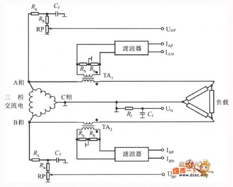
The ADE7752circuit that adopts three phase three wires system triangle connecting laws is shown as below. only in this case use the two voltage input and current input ports of ADE7752. The active power caculated by the ADE7752 has nothing to do with the gateway it chosen.as the gateway chosen. (View)
View full Circuit Diagram | Comments | Reading(828)
35w set -top -box switching supply circuit diagram
Published:2011/5/11 4:16:00 Author:Ecco | Keyword: 35w supply , set -top -box switching
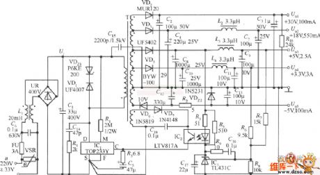
The 5 roads voltage of 35w set -top -box switching supply circuit diagram are distinguished as: Uo1(+30 V, 100 ma), Uo2(+18 V, 550 ma), Uo3(+5 V, 2.5 A), Uo4(+3.3 V, 3 A), Uo5.(-5 V, 100 ma). Among them, +5 V and + 3.3 Vare main output, the rest of allare assisting output. When the swaping input voltage u=220(1 ± 15%) V, the total output power ofswitch reaches 38.5 W, if adopting breadth range voltage input(u=85~265 V), the total outputreduces 25 W. It can be used as the power supply of box(Set ― top Box), video recorder(VCR) , shoot video recorder(CVCR) and DVD machine. The power supply of machine set -top -box switching is higher than 77%, and it has the function of undervoltage and overvoltage protection. (View)
View full Circuit Diagram | Comments | Reading(5624)
Simple light-operated street lamp circuit diagram(6)
Published:2011/6/28 2:35:00 Author:Ecco | Keyword: Simple , light-operated , street lamp

The chart shows the simple light-operated street lamp circuit with better performance , and it can be used in the automatic control of street lamps in residential district. The controlled street light can use incandescent bulbs or energy-saving fluorescent lamps.
(View)
View full Circuit Diagram | Comments | Reading(1596)
Capacitive dimmer switch circuit (1)
Published:2011/6/28 2:36:00 Author:Ecco | Keyword: Capacitive , dimmer switch
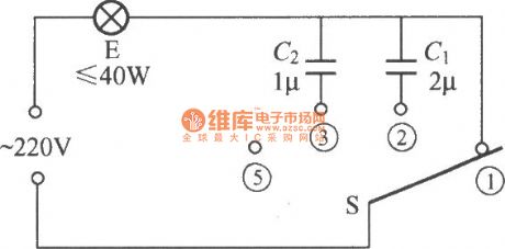
Capacitive dimmer switch circuit is shown as the chart, it uses the principle of capacitors having AC capacitance. When S is located in the position in the figure, E bulb emits normal light, that is the maximum brightness; when it is switched to the position ②, as the 2μF capacitor is connected in series C1, light intensity of E decreases; when it is switched to the position ③, because of C2
(View)
View full Circuit Diagram | Comments | Reading(953)
Capacitive dimmer switch circuit (2)
Published:2011/6/28 2:35:00 Author:Ecco | Keyword: Capacitive , dimmer switch
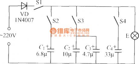
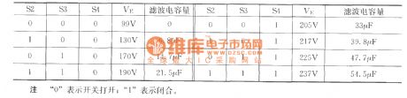
The circuit described as the chart is the dimmer switch circuit which uses the capacitor discharging principle, and it is suitable for incandescent light, and it has no interference effect on radio, television and other appliances. The principle of the circuit is shown as the chart. The relationship of voltage VE across the lamp and the switch combination is shown as the following table:
(View)
View full Circuit Diagram | Comments | Reading(733)
Electric sewing machine no load energy saver 2
Published:2011/6/30 0:49:00 Author:Nicole | Keyword: sewing machine, no load energy saver
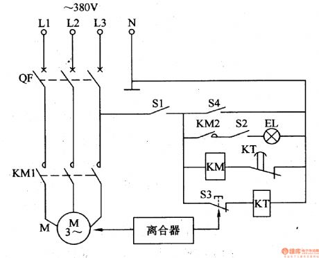
The electric sewing machine no load energy saver circuit is composed of low high circuit breaker QF, control switch S1, light switch S2, S4, footage switch S3, AC contactor KM and time relay KT, it is shown in the figure 8-4.
When it is used, the low high circuit breaker QF is turned on, then S1, S2 are turned on, the sewing worker puts her feet on the clutch pedal, the foot switch S3 is cut off, KM pulls in, its normally open contact KM1 is connected, the motor M starts running, light EL turns on, the work can start to sew.
(View)
View full Circuit Diagram | Comments | Reading(783)
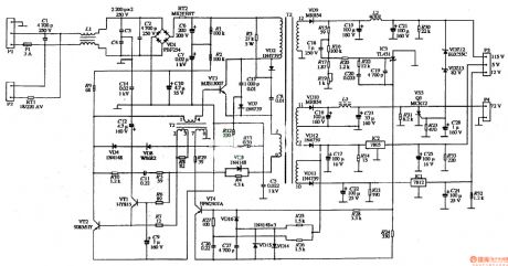
The power supply circuit of CTX-C15 VGA high resolution color display
Published:2011/5/12 2:20:00 Author:Ecco | Keyword: VGA, high resolution , color , display, power supply
View full Circuit Diagram | Comments | Reading(846)
50Hz high-precision time base signal source(CD4060)
Published:2011/5/12 2:24:00 Author:Ecco | Keyword: 50Hz , high-precision , time base, signal source
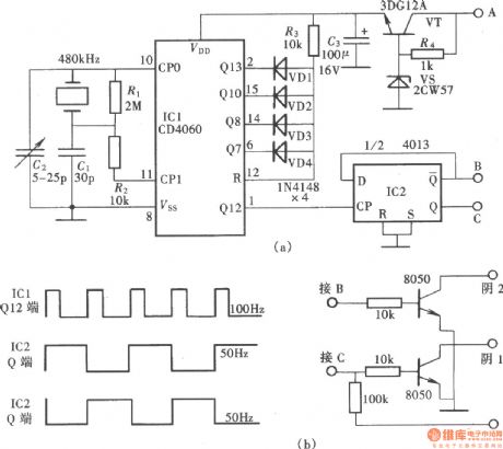
In some of the early production of the digital electronic clocks with AC power supply, the 50Hz AC power frequency is used as a second time base after fractional frequency because of structure. As the frequency of AC power will always has a certain bias, this small deviation will cause the large deviation between the real time and clock over time. In order to eliminate this bias, amateur enthusiasts make a variety of 50Hz high-precision time base circuits. The most using is the circuit composed of CD4060, it is shown as the chart.
(View)
View full Circuit Diagram | Comments | Reading(6031)
Frequency signal tracking circuit (PLL circuit) composed of CD4046
Published:2011/5/12 2:16:00 Author:Ecco | Keyword: Frequency signal , tracking , PLL
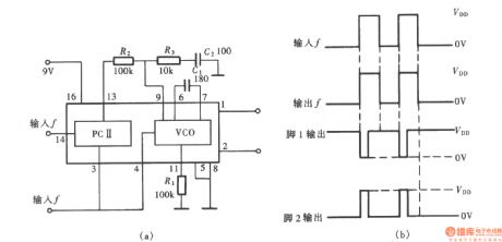
Frequency signal tracking circuit is the phase-locked loop circuit, which is one of the basic application circuit of CD4046. The circuit shown as the chart and composed of CD4046 is a PLL circuit, and it can capture and track the input signal with the input frequency in l00~100kHz . (View)
View full Circuit Diagram | Comments | Reading(7170)
Ten blocks frequency signal generator(CD4011、CD4017)
Published:2011/5/12 2:05:00 Author:Ecco | Keyword: Ten blocks, frequency, signal generator
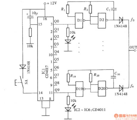
Usually, we use the general-purpose frequency signal generator which is designed as the entire frequency range with a continuous adjustment approach. However, in actual use, we only use a few test frequency. Here the frequency signal generator has been designed ten commonly used fixed-frequency gears,and you can choose the gear according to the need. The frequency signal generator consists of digital gear selector switch and ten fixed frequency signal generator, it is shown as the chart.
(View)
View full Circuit Diagram | Comments | Reading(1650)
Transistor ringing current generator
Published:2011/5/12 2:07:00 Author:Ecco | Keyword: Transistor, ringing current generator
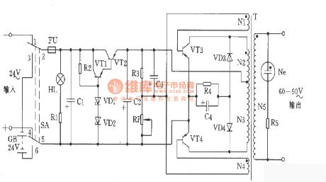
Transistorringing current generatorchanges 24V DC into 60 ~ 90V AC ringing voltage for the supply of communications equipment, such as carrier, high-frequency terminals, wired telephone. 1. Technical performance (1) Input power: DC 24V ± 10%; (2) Rated output: 60 ~ 90V AC; (3) Frequency: 20Hz ± 5Hz; (4) Working conditions: temperature +5 ℃ ~ +40 ℃, ≤ 80% relative humidity environment, it can continuous work in 24 hours. 2. Choosing components: Cl, C2 use 1000μ/50V capacitor, C3 uses 200μ/50V capacitor, C4 is 10μ/150V capacitor. Resistor Rl is 200Ω, 1/2W, R2 is 1kΩ, lW, R3 is 3.6kΩ, 2W, R4 is 5.1kΩ, lW, R5 is 20kΩ, 1W, all of them are metal film resistors. Potentiometer RP is 33Ω, lW. Zener VDl is 2CW75, VD2 is 2CW73. Diode VD3, VD4 are 2CPl3. Transistor VTl is 3AD638, VT2, VT3 are 3AD30C. HL lights is XDX-24V, 0.5A, neon uses NH0-4C (60V, lmA). Power switch SA is KN3-3 (DPDT). Insurance FU is BGXP-1 2A fusion tube. Transformer T uses silicon material with core cross-sectional area in 38 × 45mm2. Nl, N4 are Φ0.25mm 39 high-strength magnet wires with winding turns, N2, N3 use enameled high strength Φ0.49mm with l89 turn, they are two-lane and winding. N5 uses enameled Φ0.35mm high strength wire with 840 turns.
(View)
View full Circuit Diagram | Comments | Reading(949)
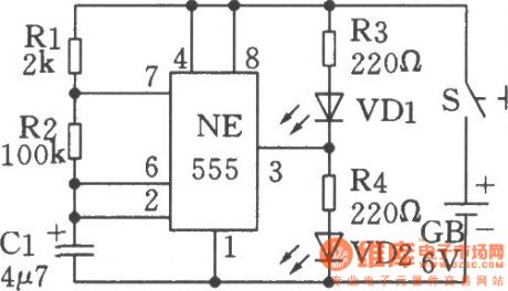
Low frequency oscillator (flashing shine circuit) circuit 1 made by 555 time-base circuit
Published:2011/5/12 2:03:00 Author:Ecco | Keyword: Low frequency, oscillator, flashing, shine , 555, time-base circuit
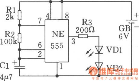
The chart shows a flashing shine circuit, and when the circuit works, twolight-emitting diodes will shine simultaneously. The working principle of the circuit is similar to 555 audio oscillator, the difference is that the capacity of capacitor Clis increased to 4.7μF. Therefore, the circuit's oscillation frequency is very low, the changing rate of potential on pin 3 of NE555 is low. When the output of pin 3is inhigh level, the light-emitting diode VDl, VD2 are lit at the same time. When the output of pin 3is inlow level, the light-emitting diode VDl, VD2 turns off.In the circuit, when the resistance of R3 is higher, the brightnessis smaller; or resistance of R3 is lower, the brightnessis greater. Note:theresistance of R3 should not be too small, otherwise the current flowing through the light-emitting diodes is too high, the power consumption is higher,it will have negative impact on thelight-emitting diode, or even it is burned. Typically, the current flowing through the LED can be controlled between 10 ~ 20mA.
(View)
View full Circuit Diagram | Comments | Reading(1108)
Electric sewing machine no load energy saver 1
Published:2011/6/29 23:02:00 Author:Nicole | Keyword: sewing machine, no load energy saver
The electric sewing machine no load energy saver circuit is composed of DC regulated power supply circuit, sensor control circuit and master control circuit, it is shown in the figure 8-3.
The DC regulated power supply circuit is made of hypotension capacitor C1, discharge resistor R1, bridge rectifiers UR, filter capacitor C2, C3, current limiting resistor R2 and steady voltage diode VS.
The sensor control circuit consists of magnet which is fixed on the sewing machine clutch operating lever and Hall sensor integrated circuit IC, resistors R3, R4, capacitor C4, transistor V, diode VD, LED VL and relay K.
(View)
View full Circuit Diagram | Comments | Reading(2521)
Low frequency oscillator (flashing shine circuit) circuit 2 made by 555 time-base circuit
Published:2011/5/12 2:01:00 Author:Ecco | Keyword: Low frequency , oscillator, flashing, shine , 555 , time-base circuit
The chart shows the flashing shine circuit based on 555 circuit,and when the circuit works, two light-emitting diodes will shine
alternately. The working principle: The NE555 time-base circuit and Rl、R2、Cl form a low frequency oscillator. When the circuit starts oscillation, the level of pin 3 in theNE555 time-base circuitis variable. When pin 3 is in high level, VD1 loses power and doesn't emit light, VD2 gets power and emits light; when pin 3 is inlow level, VD2 loses power and doesn't emit light, VD1 gets power and emit light. So two light-emitting diodes will shine alternately. When doing the circuit, the diodes could choose red, green or yellow, the difference will be more marked.
(View)
View full Circuit Diagram | Comments | Reading(661)
Pulse and pulse train generator composed of CD4093
Published:2011/5/17 4:01:00 Author:Ecco | Keyword: Pulse, pulse train , generator
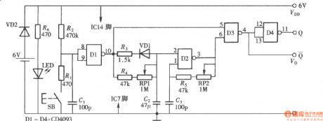
Pulse and pulse train generator is mainly composed of a CD4093 four - two input terminals Schmitt trigger and a button switch. When people press the button, the circuit outputs a single pulse, when people press the button for a period of time, the circuit will output the pulse train. The circuit is shown as the chart. The circuit consists of push button switch, input control circuit, pulse oscillator and pulse output circuit.
(View)
View full Circuit Diagram | Comments | Reading(2711)
DC regulated power supply circuit diagram with 2A output
Published:2011/5/17 4:01:00 Author:Ecco | Keyword: DC , regulated power supply , 2A output
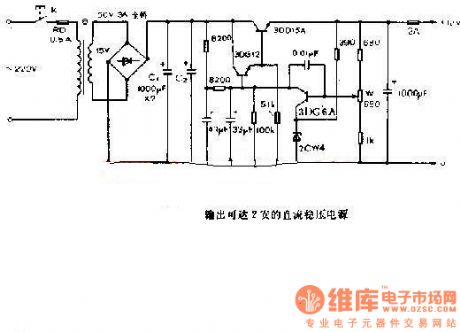
Thisis theDC regulated power supply with constant output in 2A. It is suitable for adjusting voltage of the electrical equipments and TV with 2A current and 12V voltage. The chart shows the circuit:
(View)
View full Circuit Diagram | Comments | Reading(2758)
Long cycle on / off multivibrator
Published:2011/5/17 4:02:00 Author:Ecco | Keyword: Long cycle , on , / off , multivibrator

The multivibrator composed of 555 timer IC can adjust the frequency and duty cycle independently, but if the on / off cycle is very long, it needs a large capacity capacitor. The circuit shown as the chart can adjust the on / off cycle flexibly without using large capacitors, and the longest period can reach several hours. It uses CD4020 14-stage binary counter to count the output frequency, the two output terminals Ql4 of CD4020 will rise and fall to connect to the edges Rl and R2, it can output separate off-cycle and on-cycle. The output end Q1 can be used to indicate the continuous cycle. If R2 = 100k time, Ton ≈ 5 minutes; if Rl = 1M time, Toff ≈ 50 minutes.
(View)
View full Circuit Diagram | Comments | Reading(2511)
| Pages:1537/2234 At 2015211522152315241525152615271528152915301531153215331534153515361537153815391540Under 20 |
Circuit Categories
power supply circuit
Amplifier Circuit
Basic Circuit
LED and Light Circuit
Sensor Circuit
Signal Processing
Electrical Equipment Circuit
Control Circuit
Remote Control Circuit
A/D-D/A Converter Circuit
Audio Circuit
Measuring and Test Circuit
Communication Circuit
Computer-Related Circuit
555 Circuit
Automotive Circuit
Repairing Circuit