
Circuit Diagram
Index 1528
Differential Input Amplifier Circuit With Common-Mode Voltage Up To ±100V
Published:2011/7/16 8:59:00 Author:Robert | Keyword: Differential, Input, Amplifier, Common-Mode Voltage, ±100V
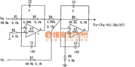
The picture shows the differential input amplifier circuit with common-mode voltage up to ±100V. In practical applications, sometime it needs the amplifier to have high common-mode voltage (±100V). For enhancement of this feature, it offen needs to sacrific some other features. The differential input amplifier circuit, which could achieve that the common-mode voltage is up to ±l00V, is shown in the picture. This circuit's voltage gain is only equal to 1. The circuit uses two common integrated single operational amplifiers 301.
The table shows the 301 integrated operational amplifier's main parameters (typical value). (View)
View full Circuit Diagram | Comments | Reading(768)
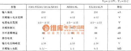
Differential Output Amplification Circuit
Published:2011/7/17 8:21:00 Author:Robert | Keyword: Differential, Output, Amplification
The picture shows the differential output amplification circuit. (View)
View full Circuit Diagram | Comments | Reading(609)
Class AB Amplification Complementary Symmetry Circuit
Published:2011/7/15 20:08:00 Author:Robert | Keyword: Class AB, Amplification, Complementary, Symmetry
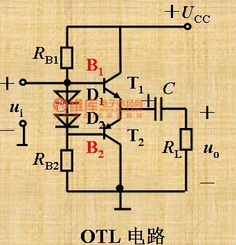
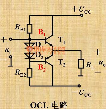
The picture shows the class AB amplification complementary symmetry circuit.
The circuit picture shows the OTL circuit. The second picture shows the OCL circuit.
These circuits have the following features:
(a)By adding RB1, RB2 it provides a certain bias current to avoid the crossover distortion.
(b)By adding diode D1, D2 it could make the B1 point and B2 point keep different voltage level in static mode and it could send the ui signal to the B1, B2 points successfully in dynamic mode. (View)
View full Circuit Diagram | Comments | Reading(924)
The inverter circuit 1
Published:2011/7/16 4:17:00 Author:Christina | Keyword: inverter
View full Circuit Diagram | Comments | Reading(1342)
The inverter circuit 10
Published:2011/7/16 4:17:00 Author:Christina | Keyword: inverter
View full Circuit Diagram | Comments | Reading(4104)
Sensor circuit 102: carbon monoxide sensor circuit
Published:2011/7/14 21:07:00 Author:zj | Keyword: Sensor circuit, carbon monoxide sensor
View full Circuit Diagram | Comments | Reading(2356)
Sensor circuit 103: Ion detector circuit
Published:2011/7/14 21:18:00 Author:zj | Keyword: Sensor circuit, Ion detector circuit
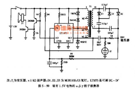
Note: T1 is transformer, *1 8Ω speaker; D1, D2, D3 are MUR1100; U1 neon. LT1073 is adjustable DC-D
Figue 5-99 α, β, γ particle detector with 1.5V battery (View)
View full Circuit Diagram | Comments | Reading(2689)
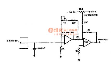
Sensor circuit figure 108: pH sensor measuring circuit
Published:2011/7/14 21:30:00 Author:zj | Keyword: Sensor circuit, pH sensor measuring
View full Circuit Diagram | Comments | Reading(1946)
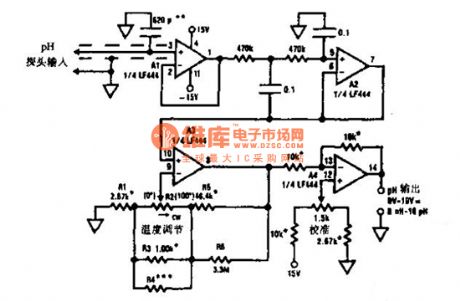
Sensor circuit figure 109: pH sensor measurement compensation circuit
Published:2011/7/14 21:32:00 Author:zj | Keyword: Sensor circuit, pH sensor, measurement, compensation
View full Circuit Diagram | Comments | Reading(1484)
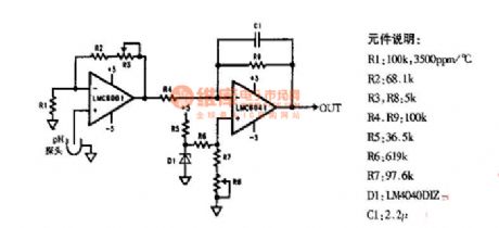
Sensor circuit figure 110: pH probe amplification circuit
Published:2011/7/14 21:34:00 Author:zj | Keyword: Sensor circuit, pH probe, amplification circuit
View full Circuit Diagram | Comments | Reading(2620)
The 485 interface circuit diagram
Published:2011/7/14 21:36:00 Author:zj | Keyword: The 485 interface
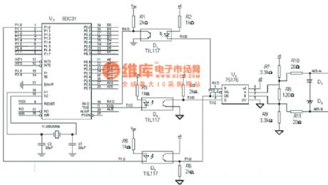
View full Circuit Diagram | Comments | Reading(1133)
Homemade VGA-TV interface circuit diagram
Published:2011/7/14 21:39:00 Author:zj | Keyword: Homemade, VGA-TV interface
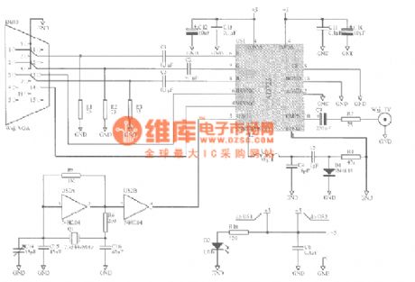
View full Circuit Diagram | Comments | Reading(2323)
Video amplifier circuit
Published:2011/7/14 22:02:00 Author:zj | Keyword: Video amplifier
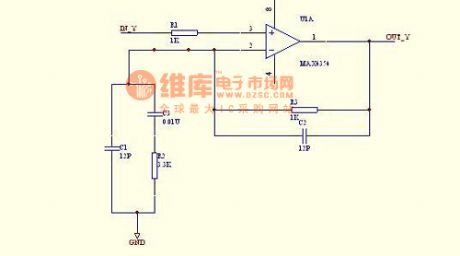
View full Circuit Diagram | Comments | Reading(616)
Varistor circuit diagram
Published:2011/7/14 22:04:00 Author:zj | Keyword: Varistor circuit
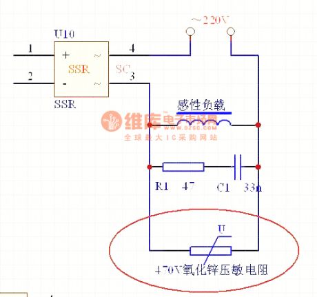
View full Circuit Diagram | Comments | Reading(3330)
[165V.HID.PWM] half bridge driver module
Published:2011/7/16 4:01:00 Author:Christina | Keyword: half bridge, driver module
![[165V.HID.PWM] half bridge driver module](/uploadfile/ic-circuit/s20117164117737.gif)
View full Circuit Diagram | Comments | Reading(3210)
50W DC converter
Published:2011/7/15 23:53:00 Author:Christina | Keyword: 50W, DC, converter
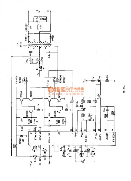
The control, adjustment, surveillance, and other functions are beared by the TDA4700, the output controls the push-pull stage, and the voltage is output by the transformer.
The main technical data:
Output voltage U1:20-28V(typical value:24V)Output voltage U2:0-5.25V(typical value:5V)Output current I2:0-10ALoad voltage adjustment rate:0.4%efficiency:72%Positive loss PVD:0.9WSwitch loss PVS=0.4WTotal loss PVD+PVS=1.3W.
(View)
View full Circuit Diagram | Comments | Reading(1016)
Transistor Relay Time-Delay Closing Circuit
Published:2011/7/17 0:56:00 Author:Robert | Keyword: Transistor, Relay, Time-Delay, Closing
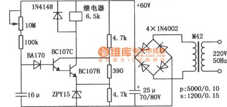
The picture shows the transistor relay time-delay closing circuit. When it is connected to the power supply, the voltage on the 16uF capacitor would be 0V and the two triodes are all off and the relay has no action. As the 16uF capacitor charging, after some time, the voltage on it would get to high voltage level and the two triodes are all turned on and the relay would be closed after the delay time. The delay time could be 60s. The length of delay time can be adjusted by the 10MΩ resistor. (View)
View full Circuit Diagram | Comments | Reading(771)
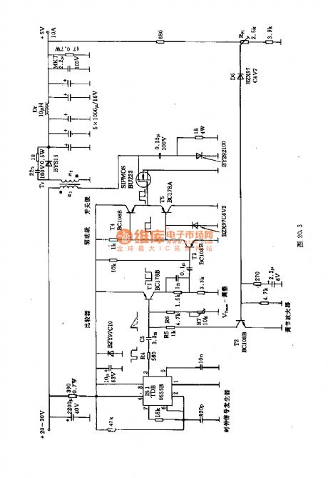
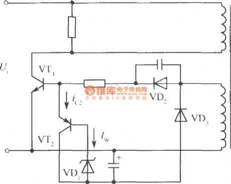
Ringing type switching power supply constant current driving circuit
Published:2011/7/15 23:18:00 Author:Christina | Keyword: Ringing type, switching, power supply, constant current, driving circuit
In the ringing type switching power supply, the power loss of the driving circuit which supplies the base current to the switching transistor is very large. The voltage UB of the transformer coil NB must ensure the minimum input voltage of the switching transistor to make the fully conduction, and the voltage UB is proportional to the input voltage Vi. When the Vi increases, the driving current Id will increases too, but the base resistance Rb increases the power loss that has the square relationship with the increasing part of Id.
When the driving current ID is increasing, the voltage stabilization diode subcircuit current will increase too, and this will cause the oscillation problem, in a certain period of time, the switch works, and in the next period of time, the switch stops working.
(View)
View full Circuit Diagram | Comments | Reading(700)
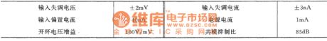
Single Operational Amplifier Basic Subtraction Circuit Composed Of LM158
Published:2011/7/16 21:02:00 Author:Robert | Keyword: Single, Operational Amplifier, Basic, Subtraction
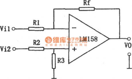
The picture shows the single operational amplifier basic subtraction circuit.
To avoid the error caused by the bias current, it is required that the external circuit total resistance value of the operational amplifier's two input ports should be balanced.
This circuit uses the element of LM158. It is a single-chip high-gain dual operational amplifiers which would work under a wide range of single power supply. Its power current would be small and would have no relations to the power voltage. The LM158's main parameters are listed in the table. (View)
View full Circuit Diagram | Comments | Reading(924)
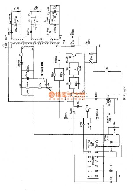
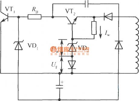
Ringing type switch power supply power expansion method
Published:2011/7/15 22:54:00 Author:Christina | Keyword: Ringing type, switch, power supply, power expansion
In the simple ringing current-limit power supply circuit, in order to make the output voltage stable, we need to connect the voltage-regulator diode with the base electrode of the switching transistor VTl, so the output voltage can not be adjusted. In addition, if you want to increase the output power, you need to increase the driving current. At this time, if you decrease the output current, the subcircuit current of the voltage-regulator diode will increase. This will change the voltage stabilization value of the voltage stabilization diode, even more than the allowable value of the voltage stabilization diode. So in order to improve the output power, we can use the method of add a current expansion transistor which is as shown in the figure.
(View)
View full Circuit Diagram | Comments | Reading(664)
| Pages:1528/2234 At 2015211522152315241525152615271528152915301531153215331534153515361537153815391540Under 20 |
Circuit Categories
power supply circuit
Amplifier Circuit
Basic Circuit
LED and Light Circuit
Sensor Circuit
Signal Processing
Electrical Equipment Circuit
Control Circuit
Remote Control Circuit
A/D-D/A Converter Circuit
Audio Circuit
Measuring and Test Circuit
Communication Circuit
Computer-Related Circuit
555 Circuit
Automotive Circuit
Repairing Circuit