
Circuit Diagram
Index 1536
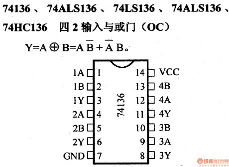
74 series digital circuit of 74136 and 74ALS136 four 2 input and nor gate(OC)
Published:2011/5/17 3:21:00 Author:Ecco | Keyword: digital circuit , four 2 input, nor gate
View full Circuit Diagram | Comments | Reading(1394)
74 series digital circuit of 74LS112A 74F112 double J - K negative edge trigger
Published:2011/5/17 3:21:00 Author:Ecco | Keyword: digital circuit , double J - K negative edge, trigger
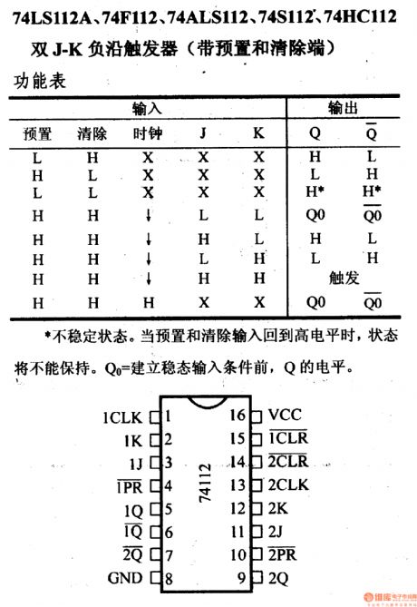
74 series digital circuit of 74LS112A,74F112 double J - K negative edge trigger( with preset and remove terminal)
(View)
View full Circuit Diagram | Comments | Reading(1552)
74 series digital circuit of 7473 and 74H73 input J - K master-slave flip-flop
Published:2011/5/17 3:22:00 Author:Ecco | Keyword: digital circuit, input J - K, master-slave flip-flop
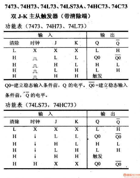
7473, 74H73,74L73, 74LS73A, 74HC73, 73C73double J - K master-slave flip-flop(with remove terminal)
The level of Qo is equal to Q before eatablishing steadystate input. (View)
View full Circuit Diagram | Comments | Reading(1998)
Motor protector 14
Published:2011/6/27 21:39:00 Author:Nicole | Keyword: Motor, protector
This motor protector circuit is composed of power supply circuit and phase failure detection protection circuit, it is shown in the figure 8-50.
The power supply circuit is made of power transformer T, rectifier diode VD3, fliter capacitor C2, current limiting resistor R4 and LED VL.
The phase failure detection protection circuit consists of resistors R1-R3, capacitor C1, diodes VD1, VD2, potentiometer RP, transistors V1, V2 and relay K.
The phase failure protection circuit's sensitivity can be changed by adjusting RP.
(View)
View full Circuit Diagram | Comments | Reading(802)
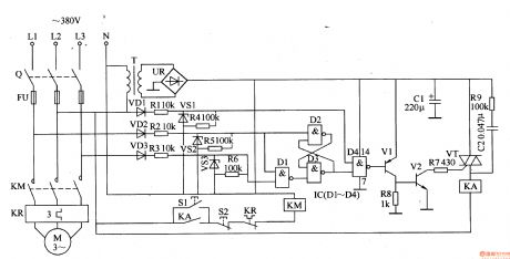
Motor protector 13
Published:2011/6/27 21:29:00 Author:Nicole | Keyword: Motor, protector

This motor protector circuit is composed of power supply circuit, phase sequence detection circuit, trigger and protection control circuit, it is shown in the figure 8-49.
The phase sequence detection circuit is made of diodes VDl-VD3, resistors R1-R6 and steady voltage diodes VS1-VS3.
The protection control circuit consists of transistors V1, V2, resistors R7-R9, capacitor C2, thyristor VT and middle relay KA.
The motor control circuit is composed of starter button S1, stop button S2, knife switch Q, fuse FU, heat relay KR and AC contactor KM.
(View)
View full Circuit Diagram | Comments | Reading(870)
Negative oxygen ion generator 1
Published:2011/6/27 23:00:00 Author:Nicole | Keyword: oxygen ion, generator
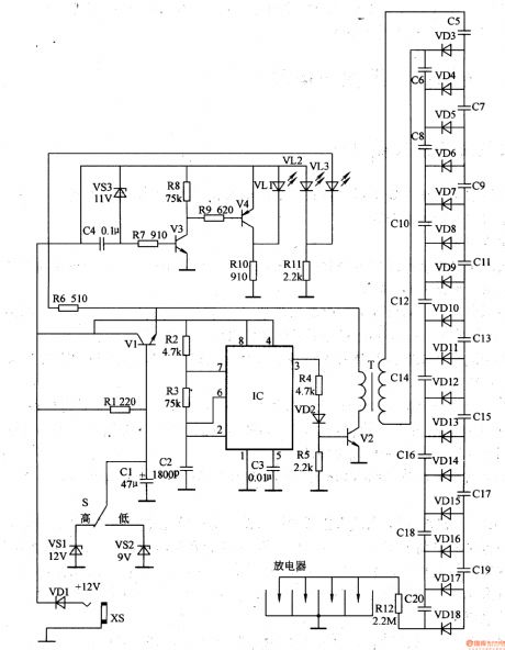
This negative oxygen ion generator circuit is composed of power supply steady voltage circuit, under voltage detection indication circuit, high frequency oscillator and high voltage generator circuit, it is shown in the figure 9-113.
The power supply steady voltage circuit is made of diode VD1, power supply regulator V1, steady voltage diodes VS1, VS2, ionization selection switch S, power supply indication LED VL2 and peripheral resistor capacitor components.
The under voltage detection indication circuit consists of transistors V3, V4, steady voltage diode VS3, under voltage indication LED VL1 and peripheral resistor capacitor components.
(View)
View full Circuit Diagram | Comments | Reading(5403)
Wireless remote control electric initiator 2
Published:2011/6/30 22:26:00 Author:Nicole | Keyword: wireless remote control, electric initiator
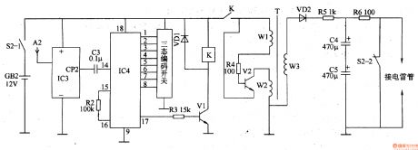
The wireless receive initiation circuit is composed of power switch S2(S2-1, S2-2), battery GB2, receiving antenna A2, wireless receive integrated circuit IC3, wireless decoding integrated circuit IC4, resistors R2-R6, capacitors C3-C5, transistors V1, V2, diodes VD1, VD2, relay K and boost transformer T, it is shown in the figure 8-28. The wireless receive control circuit is made of A2, IC3, IC4, C3, R2, R3, VDl, Vl and K, the oscillation boost circuit consists of R4, V2, T, the charge-discharge circuit is composed of VD2, R5, C4, C5, R6.
(View)
View full Circuit Diagram | Comments | Reading(583)
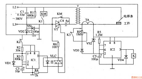
Electric welding machine no load electricity saver 3
Published:2011/6/30 20:30:00 Author:Nicole | Keyword: electric welding machine, electricity saver
The electric welding machine no load electricity saver circuit is composed of power supply circuit, delay trigger circuit and control implement circuit, it is shown in the figure 8-7.
The power supply circuit is made of knife switch Q, fuse FU, the normally open contact of AC contactor KM, electric welding machine transformer T, rectifier diode VD1, filter capacitor C2, steady voltage diode VS1 and current limiting resistor R1.
The delay trigger circuit consists of steady voltage diode VS2, VS3, potentiometer RP, resistors R2-R5, capacitor C3, diode VD2 and unijunction transistor VU.
(View)
View full Circuit Diagram | Comments | Reading(2709)
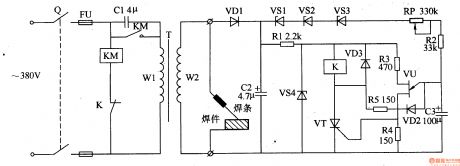
Electric welding machine no load electricity saver 2
Published:2011/6/30 20:23:00 Author:Nicole | Keyword: electric welding machine, electricity saver
The electric welding machine no load electricity saver circuit is composed of power supply circuit, pulse oscillator, monostable trigger and control circuit, it is shown in the figure 8-6.
The power supply circuit is made of depressurization capacitor C1, resistor R1, steady voltage diode VS1, rectifier diode VD2 and filter capacitor C2.
The pulse oscillator consists of time base integrated circuit IC1 and peripheral devices.
The monostable trigger is composed of time base integrated circuit IC2 and resistor R5, capacitor C5.
The control circuit is made of optical coupler VLC, relay K, AC contactor KM and TRIAC VT.
(View)
View full Circuit Diagram | Comments | Reading(3939)
Electric welding machine no load electricity saver 1
Published:2011/6/30 20:15:00 Author:Nicole | Keyword: electric welding machine, electricity saver
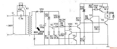
The electric welding machine no load electricity saver circuit is composed of relay drive circuit, low voltage detection control circuit, high voltage timing control circuit or voltage self-adaptive tracking regulation circuit, it is shown in the figure 8-5.
The low voltage detection control circuit is made of relay K's normally closed contact K2, steady voltage diode VS1, resistor R1 or transistor V6.
The high voltage timing control circuit consists of steady voltage diode VS2, resistors R2, R6, capacitor C2 or transistor V5.
The relay drive circuit is composed of relay K, transistors V1, V2 and diode VD3.
(View)
View full Circuit Diagram | Comments | Reading(3221)
Amproluck MB-23 PC grill microwave computer control panel
Published:2011/5/12 2:18:00 Author:Ecco | Keyword: Amproluck , PC, grill , microwave , computer , control panel
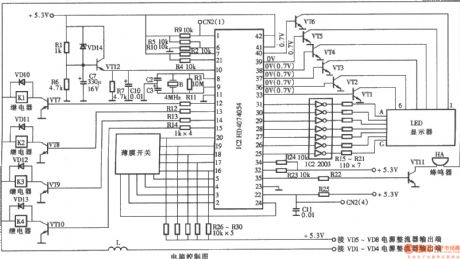
View full Circuit Diagram | Comments | Reading(755)
Amproluck WD850ES PC microwave computer control panel
Published:2011/5/12 2:17:00 Author:Ecco | Keyword: Amproluck, PC , microwave , computer , control panel
View full Circuit Diagram | Comments | Reading(764)
Electronic fly disinfestation browser
Published:2011/5/12 2:12:00 Author:Ecco | Keyword: Electronic , fly disinfestation browser
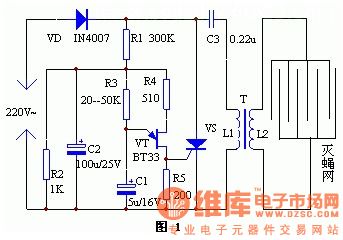
This electronic fly disinfestation browser is simple and easy to make, it is used to wipe out all flies which fly to the power grid of the device.
The circuit is shown in Figure 1. The whole device is supplied by the 220V electric supply after being rectified. R3, R4, R5, C1 and double-base diode form a relaxation oscillator, the output pulse signal is used to control the SCR's turning on and off. When SCR is in the off state, electric supply VD is rectified and charges for C3 by equivalent resistor R6 and L1. When VS is triggered and turned, C3 discharges rapidly by SCR and the equivalent resistor of L1. When the discharging current is over zero, the SCR cuts off automatically. This repeats the cycle, the secondary stage L2 of transformer gets a high pulse voltage, the voltage is applied to the power grid composed of many equidistant electrical wire, power grid sets bait to attractflies, and when they touch the grid, they will be electrocuted and then drop from the space, that realize the effect of automatically disinfestation. (View)
View full Circuit Diagram | Comments | Reading(654)
The wiring circuit diagram with single-phase watt-hour meter measuring electric power
Published:2011/5/13 3:10:00 Author:Ecco | Keyword: wiring circuit , single-phase , watt-hour meter , measuring , electric power
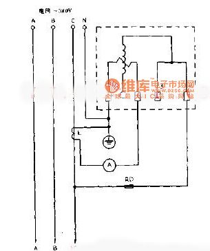
Three-phase AC power used in rural areas and plant is mainly used as electrical power for motor, it generally requires a three-phase meter. If there is only single-phase power meter, the wiring method is as the diagram, it can measure three-phase meter electricity consumption by the single-phase meter, the former single-phase watt-hour meter reading is multiplied by 3, that is the actual consumption of three-phase power.
(View)
View full Circuit Diagram | Comments | Reading(2359)
0 ~ ± 30V, 1.5A power supply circuit diagram composed of LM317
Published:2011/5/13 4:01:00 Author:Ecco | Keyword: 0, ± 30V , 1.5A , power supply
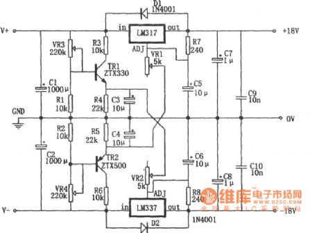
0 ~ ± 30V, 1.5A power supply circuit diagram composed of LM317 is shown as the chart. The features of the power supply can be seen from the figure, its positive and negative output voltage can be transferred to the minimum 0V. LM317 (LM337) can only be transferred to the 1.25 (-1.25) V under normal circumstances, but the adjustment end of the adjustable three-terminal is added the appropriate amount of reverse bias, the output voltage can be changed to zero by negative voltage of TH2 emitter being connected to VR1, and the positive voltage of TH1 emitter being connected to VR2. (View)
View full Circuit Diagram | Comments | Reading(5424)
8-gear constant-current current design the circuit diagram
Published:2011/5/13 4:02:00 Author:Ecco | Keyword: 8-gear, constant-current , current design
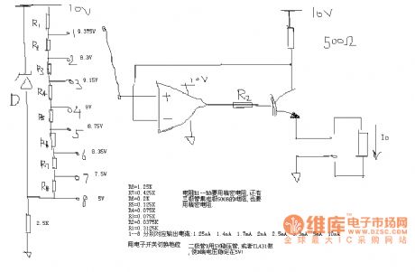
Resistors R1-R8 use precision resistors, the 500R resistors of the transistor collector also use precision resistors. Electronic switch can change the gears, the diode D uses a 5V regulator, or TL431 to make the D terminal voltage be stable at 5V.Resistors R1-R8 use precision resistors, the 500R resistors of the transistor collector also use precision resistors. Electronic switch can change the gears, the diode D uses a 5V regulator, or TL431 to make the D terminal voltage be stable at 5V.
(View)
View full Circuit Diagram | Comments | Reading(623)
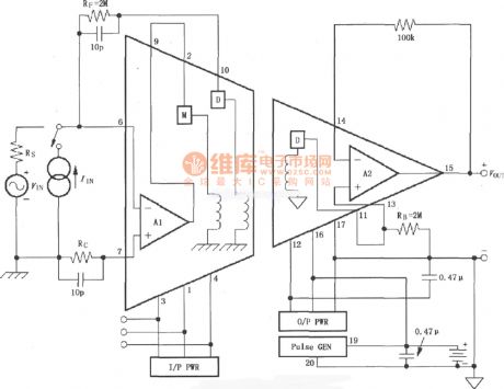
The dual-channel dual-power isolation in-phase gain circuit diagram composed of 3656
Published:2011/5/17 3:14:00 Author:Ecco | Keyword: dual-channel , dual-power , isolation , in-phase gain
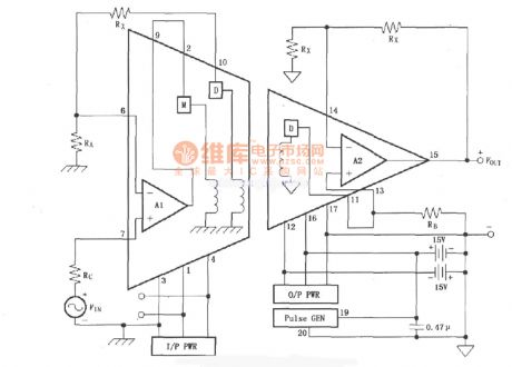
The dual-channel dual-power isolation in-phase gain circuit diagem composed of 3656 is shown as the chart. There is a bipolar power supply composed of two 15V powers being added to the pin 12,16, they have common ground which is the the ground of output level (pin 17 ), one of the two power supplies (+ V) is used as power supply for pulse generator (pin 19,20 ). Pin 12,16 do not need increase filter capacitor. The voltage isolation of the circuit: there is 3500V between the pin 3 and pin 17, pin 3 and pin 19, no voltage isolation between the pin 17 and pin 19.
(View)
View full Circuit Diagram | Comments | Reading(543)
Two-channel single-supply inverting gain circuit diagram composed of 3656
Published:2011/5/13 4:02:00 Author:Ecco | Keyword: Two-channel, single-supply , inverting gain
Two-channel single-supply inverting gain circuit diagram composed of 3656 is shown as the chart. The system uses a power supply to constitute an unipolar power supply circuit, the power ground is connected to output level ground (pin 17) to provide internal generating power for the other polarity power supply of A2, so filter is added to the pin 12. The isolated power supply can also be used for the input stage. The voltage isolation of the structure circuit: there is 3500V between the pin 3 and pin 17, pin 3 and pin 19, no isolation between the pin 19 and pin 17.
(View)
View full Circuit Diagram | Comments | Reading(556)
Bipolar noise treatment method circuit diagram composed of ISO100
Published:2011/5/17 3:29:00 Author:Ecco | Keyword: Bipolar, noise treatment method
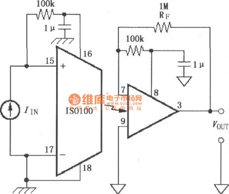
Bipolar noise treatment method circuit diagram composed of ISO100 is shown as the chart. In bipolar mode, the noise is primarily produced by the reference current source. The reference current source is added a low-pass filter to reduce the noise of the current source.
(View)
View full Circuit Diagram | Comments | Reading(493)
The monitoring (ISO122P/124, INA105) circuit diagram of battery system
Published:2011/5/17 3:23:00 Author:Ecco | Keyword: monitoring , battery system
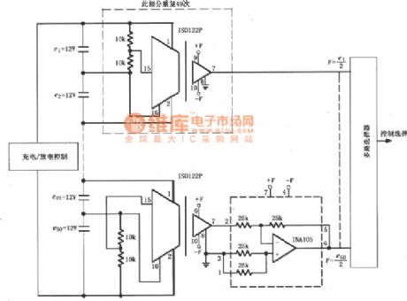
The 600V monitoring (ISO122P/124, INA105) circuit diagram of battery system composed of ISO122P/124 and instrumentation amplifier INA105, multi-route selector is shown as the chart. Circuit can detect the charging and discharging 50 pieces of 12V batteries connected in series ( the total voltage is 600V) to prevent over charge or over discharge. The input voltage of ISO122P/124 is e / 2 voltage got by the two ends of a single 12V battery divided by two 10kΩ, and it is isolated, amplified and sent to INA105. INA105 is connected as an inverting amplifier gain, it outputs e / 2 to the multiplexer, the multiplexer would controll the selection of output.
(View)
View full Circuit Diagram | Comments | Reading(615)
| Pages:1536/2234 At 2015211522152315241525152615271528152915301531153215331534153515361537153815391540Under 20 |
Circuit Categories
power supply circuit
Amplifier Circuit
Basic Circuit
LED and Light Circuit
Sensor Circuit
Signal Processing
Electrical Equipment Circuit
Control Circuit
Remote Control Circuit
A/D-D/A Converter Circuit
Audio Circuit
Measuring and Test Circuit
Communication Circuit
Computer-Related Circuit
555 Circuit
Automotive Circuit
Repairing Circuit