
Circuit Diagram
Index 1538
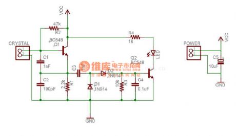
Crystal detector circuit diagram
Published:2011/5/17 4:06:00 Author:Ecco | Keyword: Crystal, detector

When buying crystals, the detector can test the quality of the high-frequency crystal. Working principle is shown as the chart, it is a Kepizi high-frequency crystal oscillator composed of VTl and sJT crystal. When itis addedsJT crystal, it can provide positive feedback loop to the base of vTl, and VT1 starts oscillation, the weak signal from oscillation will be sent to vT2 emitter by coupling capacitor c4 and drive voltage doubler detector composed of C5, C6, VDl , vD2. Then the current amplifier VT3 turns on, the light-emitting diode VD3 is lit.Among them, the emitter vT2 can provide signals to voltage doubler detector, but also IV has the effect of isolation cushion, for reaching the start-up support of VT1. When it detects crystal, sometimes the brightness of VD3 is not enough, the conclusion is not sure, you can slightly adjust the operating point R3 of transistor vT1 to achieve stable oscillation, and then adjust the gain electrical equipment RP. It needs appropriate components. Generally you do not have to adjust. Power GB uses 6F22-nc9v to cascade batteries.
(View)
View full Circuit Diagram | Comments | Reading(1067)
Medical ultrasonic atomizer 3
Published:2011/6/29 22:48:00 Author:Nicole | Keyword: ultrasonic atomizer
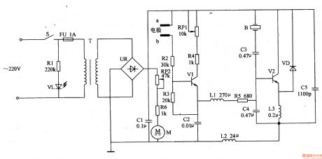
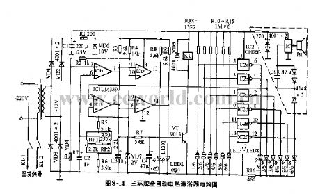
The medical ultrasonic atomizer circuit is composed of power supply circuit, on the low side of liquid level protection control circuit, ultrasonic oscillator and fan drive circuit, it is shown in the figure 9-112.
The power supply circuit is made of power supply switch S, resistor R1, power supply indication LED VL, fuse FU, power transformer T, bridge rectifiers UR and filter capacitor C1.
The low side of liquid level protection control circuit consists of liquid level detection electrodes a, b, resistors R2-R4, potentiometer RP1, potentiometer C2 and transistor V1.
(View)
View full Circuit Diagram | Comments | Reading(4556)
The unipole slab electron weighs system circuit diagram composed of ZEM series
Published:2011/5/11 4:19:00 Author:Ecco | Keyword: unipole slab , electron weighs system , ZEM series
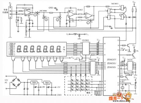
The unipole slab electronic weigh system circuit diagram composed of ZEM207 seriesis shown as below. The circuit includes the analog switch MC4066, double OPAMP TL062, a double inputs four and MC4011 in the non- portal, a seven Darlington driver UN2003(may also replace with the MC1413), a 3 wires/8 wires translator 74 HC138, a 2 Kb serial E2PROM storaging machine 24C02, three ports voltage regulations 7809, 7805. The system goes together with 7 LED displays and 4 × 4 keyboards, and display unit can select gram(g), kilo gram(kg) or ton(t). There are 8 light-emitted diode A~H, mean LW(null potential) and PZ(tare), ZL(place null) and DJ(price per unit), JE(figure ) and LC(accumulate number of times), LJ(accumulate) and LZ(accumulate weight) respectively. TXD in the chart means serial output, RXD means serial input, the BT represents low voltage indication, SW is mark of switch. U+ means connecting +9 V power supply, UCC means connecting +5 V power supply. U+L means the output voltage after returned from 9V source. (View)
View full Circuit Diagram | Comments | Reading(2680)
Headache electronic physical therapy device circuit diagram
Published:2011/5/11 4:20:00 Author:Ecco | Keyword: electronic physical therapy device
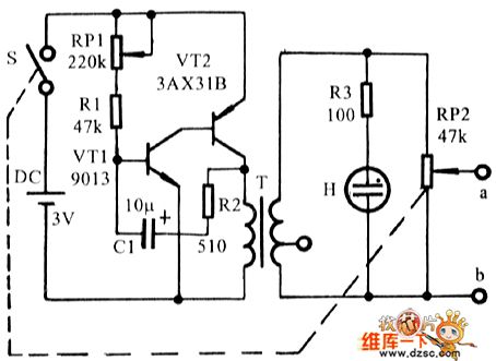
Physical therapy device circuit diagram is shown as the chart. The complementary type square-wave generator is composed of transistor VT1, VT2, and space multiplier is boosted by transformer T, then output by at a and b ports by BP2. H stands for NH - 416 type neon bulb. When the circuitry works, it will shine, indicate working status. RP1 is a type of frequency adjust potentiometer which can adjust the oscillation frequency, and we can see it from the shine of H. RP2 is a type of output strength adjust potentiometer(with switch). T could use output transformer in common transistor radios, the original 8 Ω terminal connects connentor VT2. VT1 requires that β≥100, and VT2 requires β≥50.
It needs a pair of pars of multimeter when using it, and one connects to port a of the machine, and the other one connects to port b. When paients have a headache, they could handle a par, and the other one connects to temple or frontal headache site, then open the power supply. Firstly, RP1 is put in the middle position, and make and gradually increase of RP2 until the skin contact par has the sense of acupuncture or movement. The strength of first physical shoulds not be too strong. It can be make paients feel good by adjusting PR1 to change the frequency. General physical therapy should be proper in 2 ~ 5 minutes, headache instantly disappears. If invalid, it need to be changed the frequency and appropriately increase strength, if we physiotherapy 5 minutes again, still have a headache, we will not have to try, and that explains this physical therapy device is not suitable for you.
(View)
View full Circuit Diagram | Comments | Reading(2269)
The acousto-optic circuit diagram of electron gun targeting
Published:2011/6/23 23:01:00 Author:Nicole | Keyword: acousto-optic, electron gun, targeting

The optical control monostable trigger circuit is composed of 555 and luminescence resistance RG, RP, R2, C1. When there is no light, RG is high resistance, time base circuit 555's 3 foot is low level, then LED1, LED2 which have blue light are lighted, the audio circuit does not work; when the infrared beam which is emitted by infrared electron gun hits the uminescence resistance RG of the small hole's target circuit, RG turns to low resistance, 555's 2 foot is low level(<1/3 VDD), the monostable circuit reverses, 3 foot turns to high level, then LED3, LED4(blue)are turned off, LED3, LED4(green)are turned on, at the same time, the audio circuit is triggered, it sends out sound. The acousto-optic duration time is decided by the temporary stability time of the monostable circuit, namely, td=1.1R2C1.
(View)
View full Circuit Diagram | Comments | Reading(1170)
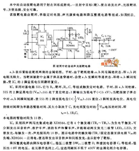
Photoelectric shooting automatic acousto-optic target-reporting circuit diagram
Published:2011/6/24 1:27:00 Author:Nicole | Keyword: photoelectric shooting, acousto-optic target-reporting
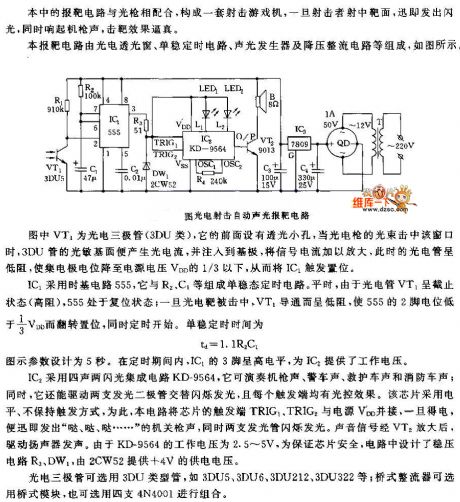
In the figure, VT1 is photoelectric triode(3DU type), there is a light hole in front of it, when the photoelectric gun's light beam hits this window, 3DU tube's photosensitive base surface will produce photocurrent, and it is injected into the base collector, the signal current is amplified, then the photoelectric tube is low resistance, the collector level is dropped below 1/3 power supply VDD, IC1 is triggered and set.
IC1 adopts time base circuit 555, the monostable timing circuit is composed of IC1 and R2, C1. Ordinarily, photoelectric tube VT1 is in off state(high resistance), 555 is in reset state; once the photoelectric target is hit, VT1 is turned on and it is low resistance, 555's 2 foot level is lower than 1/3 VDD, it is reversed and set, at the same time, the timing starts. The monostable timing time is td=1.1R2C1.
(View)
View full Circuit Diagram | Comments | Reading(546)
The hit automatic acousto-optic target-reporting circuit diagram(1)
Published:2011/6/24 1:42:00 Author:Nicole | Keyword: acousto-optic target-reporting
This target-reporting circuit is composed of target ring, monostable timing circuit, acousto-optic performance circuit and depressurization rectifier circuit, the figure is as shown.
IC1 adopts time base circuit 555, the trigger timing circuit is composed of IC1 and R1, target ring, R2, C1. Ordinarily, a and b are insulated, 555's 2 foot is high level(VDD), 555 is in reset state, 3 foot output is low level(<0.4V); when the target surface is hit by bullet, a, b are short circuit instantaneous, 555's 2 foot is low level(<1/3 VDD), 555 is set, 3 foot turns to high level. The high level duration time is the monostable temporary stability time, it is decided by the 2/3 VDD voltage time of C1 charges to reset, namely, td=1.1R2C1, the temporary stability time is 10s.
(View)
View full Circuit Diagram | Comments | Reading(567)
Preventing goods from being forgotten reminding circuit diagram
Published:2011/6/24 2:02:00 Author:Nicole | Keyword: goods, reminding
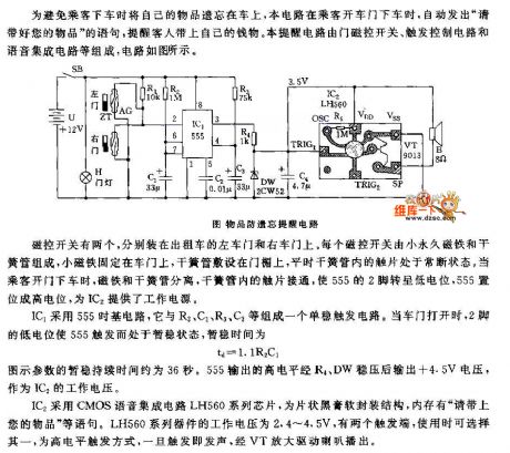
It has two magnetic control switches, they are fixed in the left and right car doors of taxi. Each magnetic control switch is composed of small permanent magnet and reed switch, the small magnet is fixed in the car door, the reed switch is set in the door head, ordinarily, the contact piece inside the reed switch is always in off state. When the passenger gets off, the magnet and reed switch are separated, the contact piece is turned on, 555's 2 foot turns to low level, 555 is set to high level, it provides IC2 with power supply.
IC1 adopts 555 time base circuit, the monostable trigger circuit is composed of IC1 and R2, C1, R3, C3. When the car door is open, 555 is tirggered by 2 foot's low level and it is in triplet state, the temporary stability time is td=1.1R2C1.
(View)
View full Circuit Diagram | Comments | Reading(517)
Infrared reflection car space reminding circuit diagram
Published:2011/6/24 3:53:00 Author:Nicole | Keyword: Infrared reflection, car space, reminding
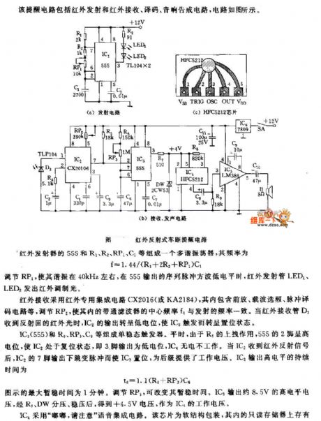
A multivibrator is composed of infrared transmitter's 555 and R1, R2, RP1, C1, the frequency is f=1.44/(R1+2R2+RP1)C1. The resonance can be about 40kHz by adjusting RP1, when the sequence pulse square wave which is outputed by 555 is low level, infrared launch tube LED1, LED2 emits infrared modulated light.
The infrared receiving adopts infrared special integrated circuit CX2016(or KA2184), it contains preamplifier, carrier frequency selection, pulse decoding circuit, the internal bandpass filter's center frequency f0 is coincidence with transmitting frequency. When the infrared launch tube D3 receives the reflected infrared light, IC2's output turns to low level, IC3 is triggered, and it turns to set state.
(View)
View full Circuit Diagram | Comments | Reading(544)
Temperature indicator
Published:2011/7/12 20:51:00 Author:zj | Keyword: Temperature indicator
View full Circuit Diagram | Comments | Reading(2354)
Intelligent pressure detection and control
Published:2011/7/12 3:02:00 Author:zj | Keyword: Intelligent, pressure detection, control
View full Circuit Diagram | Comments | Reading(690)
DAC811 external connection circuit
Published:2011/7/12 1:49:00 Author:zj | Keyword: external, connection circuit
View full Circuit Diagram | Comments | Reading(604)
Electric Water Heater Circuit 03
Published:2011/6/30 22:15:00 Author:zj | Keyword: Electric Water Heater, 03
View full Circuit Diagram | Comments | Reading(660)
Color TV pincushion correction circuit diagram 3
Published:2011/6/24 1:45:00 Author:Ecco | Keyword: Color TV , pincushion correction
The same circuits with Toshiba 2500XH pincushion correction circuit are as follow: Toshiba 2506XH, 2800XH, 2806XH etc. The field sawtooth voltage is sent to the B pole of QD03 by PD02 (3) feet, RD17, CD14, RD16, RD19, CD10. QD04 is 50Hz/60Hz switch. When the electronic switch is at 50Hz, QD04 ends, and at 60Hz, QD04 is conduction, RD19 is short, sawtooth amplitude sent to QD03B increases. QD03 is parabolic wave voltage generating tube, which can generate the concave parabolic wave voltage at C-pole output, then it is adjusted by the RD51 margin and added to the B pole of QD02, and QD02, QD01 are the parabolic wave amplifier tubes, RD50 is the line width adjustment potentiometer. (View)
View full Circuit Diagram | Comments | Reading(2390)
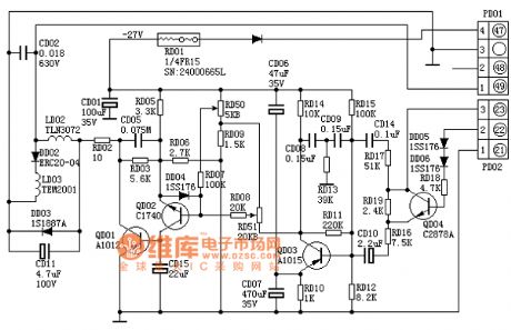
Color TV pincushion correction circuit diagram 4
Published:2011/6/24 1:49:00 Author:Ecco | Keyword: Color TV, pincushion correction
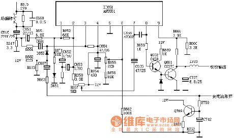
The same circuits with Hitachi CMT2988 pincushion correction circuit are as follow: Hitachi 25M8C, CMT2518, CMT2718, CMT2916, CMT2588, CMT2598, CMT2998, Furi HFC2581, 2586,2587,2986,2987 and so on. The approximately 4V (peak - peak) sawtooth voltage on two ends of R617 is added to the IC651's (1) foot by the C651, R651, then it will be made internal amplification, integration process, pin 2 will out about 2V (peak - peak) concave parabolic wave voltage. R655 is the line width adjustment potentiometer, and R657 is the school pincushion correction adjust potentiometer.
(View)
View full Circuit Diagram | Comments | Reading(1931)
Color TV pincushion correction circuit diagram 5
Published:2011/6/23 22:26:00 Author:Ecco | Keyword: Color TV , pincushion correction
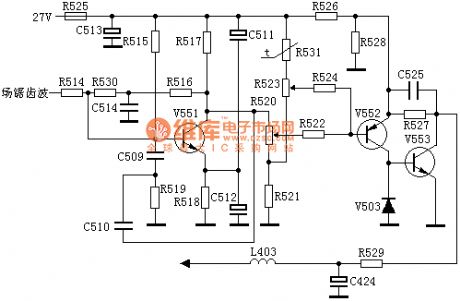
Field sawtooth wave signal is sent to the the V551's base of R514, integrated by the R516, C514, differentiated by E-B pole of C510, R519, C509, V551 to generate parabolic wave signal, and then amplified signal by V552 will be output from the collector, and directly sent to the base of V553. The parabolic wave signal output by from V553 collector is added to the negative side of V402 by R529, L403, then the V401 modulates the line deflection coil current, then the East / West pincushion distortion is corrected. The signal added on the R520 is the parabolic wave signal, and adjusting R520 can change parabolic wave signal amplitude, thus regulate the amount of the pincushion correction.
(View)
View full Circuit Diagram | Comments | Reading(1314)
Color TV pincushion correction circuit diagram 6
Published:2011/6/23 22:09:00 Author:Ecco | Keyword: Color TV , pincushion correction

The circuit is the pincushion correction circuit taken from the Venus D2918 model, and comparing with the pincushion correction circuit -1, it only has more than V951, V950 two stage amplifier, and the reason is that field sawtooth is not from sampling resistor of taken from field deflection coil but the pin of TDA8838's (46). Due to it has a lesser extent, it adds two stage amplifier.
(View)
View full Circuit Diagram | Comments | Reading(1378)
Color TV pincushion correction circuit diagram 8
Published:2011/6/23 21:26:00 Author:Ecco | Keyword: Color TV , pincushion correction
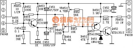
The models using pincushion correction circuit are: Samsung MC-15 movement, Venus C6418, V6458, peony 64C1, Leroy CT6388W and so on. The field sawtooth voltage is sent to pincushion correction circuit through P404 (4) feet, and R455, C454, R457 form the integral circuit to generate integration on field sawtooth wave, then it forms the convex parabolic wave voltage to add to the B pole of parabolic-wave shaping amplifier tube Q451, by the amplification, shaping the output from the C-pole 9V (peak - peak) of the concave parabolic wave voltage, and then by VR451, VR452, R464, R463, R462 component level adjustments, added to the Q453, Q452 composite pipe B-polar. VR451 is the line width adjustment potentiometer, and VR452 is a pincushion adjust potentiometer.
(View)
View full Circuit Diagram | Comments | Reading(915)
SS-D2 red light medical instrument principle and maintenance circuit diagram
Published:2011/6/27 1:35:00 Author:Ecco | Keyword: red light , medical instrument , principle , maintenance
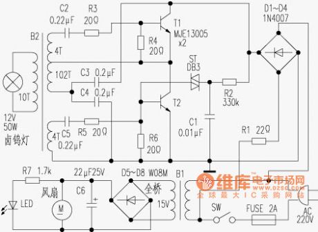
The instrument has two sets of rectifier circuit. One group is AC220V which is limited by R1, bridge rectified by D1 ~ D4, charged on C1 through R2, and when the voltage across C1 is more than turning voltage of two-way trigger diode ST, ST is conduction, so the T2 is first turned on. The coupling effect of winding B2 connected to C2, C5 in series will make T2 turn off, T1 turn on. This will enable the T1 and T2 alternately turn to build high-frequency oscillations.
(View)
View full Circuit Diagram | Comments | Reading(679)
The wiring diagram of measuring three-phase reactive power with a single-phase meter
Published:2011/6/27 1:47:00 Author:Ecco | Keyword: wiring diagram , measuring, three-phase, reactive power , single-phase meter
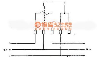
In the case of three-phase symmetric load, the wiring method in the diagram can be used to measure three-phase reactive power. Meter reading multiplied by radical sign of 3 is the three-phase reactive power.
(View)
View full Circuit Diagram | Comments | Reading(982)
| Pages:1538/2234 At 2015211522152315241525152615271528152915301531153215331534153515361537153815391540Under 20 |
Circuit Categories
power supply circuit
Amplifier Circuit
Basic Circuit
LED and Light Circuit
Sensor Circuit
Signal Processing
Electrical Equipment Circuit
Control Circuit
Remote Control Circuit
A/D-D/A Converter Circuit
Audio Circuit
Measuring and Test Circuit
Communication Circuit
Computer-Related Circuit
555 Circuit
Automotive Circuit
Repairing Circuit