
Circuit Diagram
Index 1558
Automatic Transmission Circuit Six of Soueast Lioncel
Published:2011/7/8 21:44:00 Author:Michel | Keyword: Soueast Lioncel, Automatic Transmission, Circuit Six
Automatic Transmission Circuit of Soueast Lioncel (View)
View full Circuit Diagram | Comments | Reading(668)
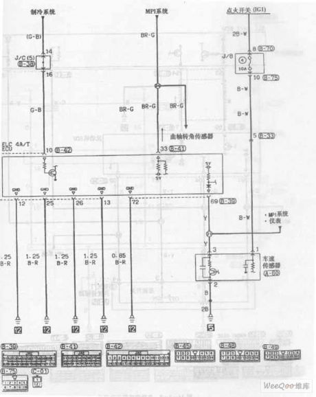
Automatic Transmission Circuit Seven of Southest Lioncel
Published:2011/7/8 21:34:00 Author:Michel | Keyword: Southest Lioncel , Automatic Transmission, Circuit Seven

Automatic Transmission Circuit of Southest Lioncel (View)
View full Circuit Diagram | Comments | Reading(506)
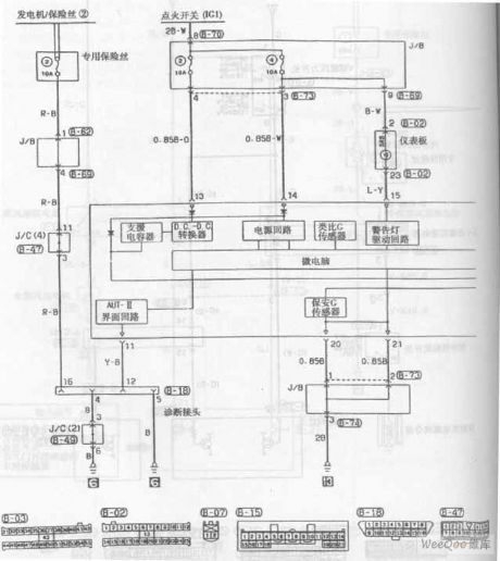
Air Bag System Circuit Two of Soueast Lioncel
Published:2011/7/9 23:09:00 Author:Michel | Keyword: Soueast Lioncel, Air Bag System, Circuit Two
Air Bag System Circuit of Soueast Lioncel (View)
View full Circuit Diagram | Comments | Reading(833)
Air Bag System Circuit One of Soueast Lioncel
Published:2011/7/9 23:09:00 Author:Michel | Keyword: Soueast Lioncel, Air Bag System, Circuit One
Air Bag System Circuit of Soueast Lioncel (View)
View full Circuit Diagram | Comments | Reading(859)
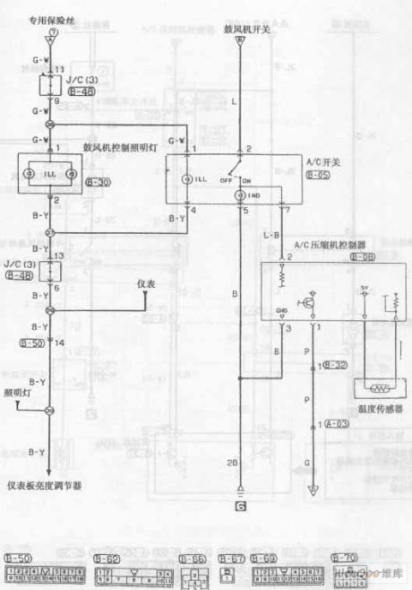
Air-conditioning Circuit Three of Soueast Lioncel
Published:2011/7/9 23:10:00 Author:Michel | Keyword: Soueast Lioncel, Air-conditioning Circuit Three
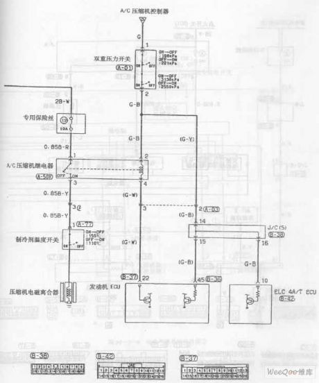
Air-conditioning Circuit of Soueast Lioncel (View)
View full Circuit Diagram | Comments | Reading(769)
Push-pull Type DC/DC Converter Circuit
Published:2011/7/7 16:20:00 Author:Michel | Keyword: Push-pull Type, DC/DC, Converter Circuit
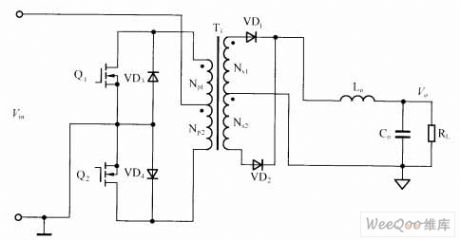
The push-pull type DC/DC converter circuit is shown as above.Among them,transformer T1 acts as isolation and energy transmission.When switch tube Q1 turns on,transformer T1's windings works and it couples with vice side Ns1 winding.When switch tube Q1 turns off,Np1 releases energy to Ns1 and vice versa.The vice edge of rectifier circuit on output end is composed of flow inductor Lo and VD1, VD2.In the circuit design,both ends of switch tube should set RC absorbing circuit to the peak surge which is produced when the switch tube turns off.
Picture:Push-pull Type DC/DC Converter Circuit
(View)
View full Circuit Diagram | Comments | Reading(4364)
LX5104 Infrared Coding Circuit
Published:2011/7/1 8:03:00 Author:Michel | Keyword: Infrared, Coding Circuit
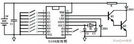
LX5104 Infrared Coding Circuit (View)
View full Circuit Diagram | Comments | Reading(1190)
TL499A switch regulator, main features and pin of DC-DC circuit and power supply monitor
Published:2011/7/10 22:21:00 Author:Lucas | Keyword: switch regulator, main features , pin , DC-DC circuit , power supply monitor
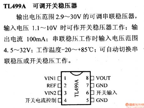
TL499A adjustable switch regulator
It is the adjustable series regulator with output voltage range in 2.9 ~ 30V, when input voltage is 1.1 ~ 10V, it can work as switching regulator; output current is 100mA; the input voltage range is 4.5 ~ 32V when it works as series regulator; Operating Temperature is -20 ~ + 85 ℃; series regulator and switching regulator can be automatically converted.
(View)
View full Circuit Diagram | Comments | Reading(670)
Dual TV and radio signal generator
Published:2011/7/6 5:00:00 Author:Lucas | Keyword: Dual , TV , radio , signal generator
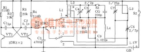
The signal generator circuit shown in the chart is simple and easy to make. This signal generator can be used as launching grid television image test signal and medium wave band radio test signals. Component selection: RC components, transistor . The specific data is shown as the chart. The power source uses a NO.5 battery, Sl is 2 × 2 small DPDT switch, and S2, S3 are the ordinary small switches . L3 is made by Φ1.5mm silver-plated copper wire winded with 4 turns, and in the the tap of the first turn, the hollow coil diameter is 1 cm.
(View)
View full Circuit Diagram | Comments | Reading(1254)
Spinner Weft feelers circuit diagram
Published:2011/6/12 22:59:00 Author:Lucas | Keyword: Spinner , Weft feelers
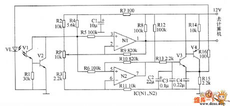
The spinner Weft feelers circuit consists of the optical signal amplifier and LED driver circuit, the circuit is shown as the chart. Optical signal detection amplifier circuit is composed of the infrared phototransistors V1 and V2, resistors R2 ~ R5 and R7 ~ R9, potentiometer RP, capacitor C1 and the N1 which is inside of the operational amplifier integrated circuit IC (N1, N2). LED driver circuit is composed of infrared light-emitting diode VL, transistors V3, V4, resistor sR2 ~ R4, R6, R10 ~ R16, potentiometer RP, capacitors C2 ~ C4 and the op amp N2 which is inside of the IC. R1 ~ R15 select 1/4W metal film resistors; R16 uses 1W metal resistor. RP uses small synthetic carbon potentiometer or variable resistor.
(View)
View full Circuit Diagram | Comments | Reading(1022)
Motor protector circuit diagram 9
Published:2011/6/13 23:38:00 Author:Lucas | Keyword: Motor protector

The motor protection circuit is composed of the start control circuit, phase detection circuit and protection implementation circuit, the circuit is shown as the chart. Control circuit is composed of starter button S2 and stop button S1 and so on. Phase failure detection circuit consists of the current transformer coil TA, rectifier diode VD1, resistor R1, capacitor C and potentiometers RP1 and RP2 and so on. Protection implementation circuit is composed of the transistors V1 ~ V3, relay K, AC contactor KM and other components. Pressing the start button S2 (S2a and linkage 52b) will make the AC contactor KM and its normally open contacts (moving together contact) KM1 ~ KM4 pull in, the motor M operates to generate 1.2V induced voltage in ⒕, the voltage is rectified by VD1 to make V2 be saturated conduction. At this point, the 52b is off, V1 stops, V3 turns on, relay K pulls in and works, its normally open contact Κ is connected, hands being away the start button S2 will maintain the normal operation of motor M.
(View)
View full Circuit Diagram | Comments | Reading(2284)
The gas limiting alarm miner lamp circuit diagram 1
Published:2011/7/6 22:06:00 Author:Lucas | Keyword: Gas limiting, alarm , miners lamp
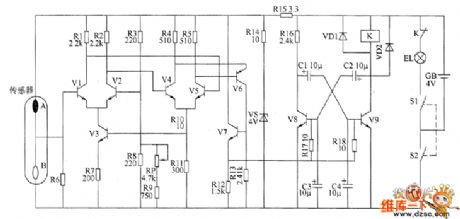
The gas limiting alarm miner's lamp circuit is composed of the detection amplifier circuit, and the circuit is shown as the chart. RP uses synthetic carbon potentiometer. C1 ~ C4 select aluminium electrolytic capacitor with the withstang voltage being more than 6.3V. VD1 and VD2 use 1N4007 or 2CP22 silicon rectifier diodes. VS selects 2CW11 silicon regulator diode. V1 ~ V5 and V7 select 59013 or 3DK4 silicon NPN transistors; V6 uses 59012 or 3CG21 silicon PNP transistor; V8 and V9 select 58050 silicon NPN transistors. K uses 4099 or JRC-5M DC relay. The sensor uses carrier catalytic gas sensor. Power switch S, miner's lamp EL, battery CB are the accessories of the original miner's lamp.
(View)
View full Circuit Diagram | Comments | Reading(689)
Application Circuits of NCP5602 and NCP5612
Published:2011/6/14 12:57:00 Author:Michel | Keyword: Application Circuits
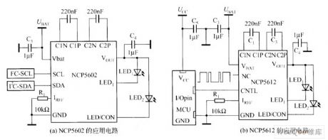
Gradual brightness changes is mainly applied to create the theatre type illuminating effect when portable electronic devices get started or closed.At startup when backlit current will be gradually amplified to 20mA in a predetermined time interval in stepping way and it will be gradually reduced when it gets colsed.Microprocessor sends different frequencies PWM signals to LED drivers' end and the LED current is increased or reduced through many stepping ways in a time interval,which achives the effects.This method shortcoming is that it consumes real-time processor,for example,this happens on NCP5602 and NCP5612's LED driver chips. (View)
View full Circuit Diagram | Comments | Reading(540)
LED Circuit of MAX6958/MAX6959 Driver
Published:2011/6/15 4:43:00 Author:Michel | Keyword: Driver, LED Circuit
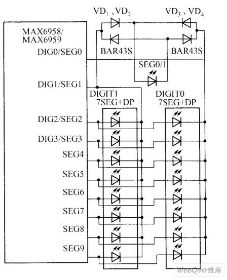
AX6958/MAX6959 is a four bit and 9 sections driver.MAX6958/MAX6959 uses six PWM(64 rank) brightness control technology, which can adjust all the average working current of LED at the same time.The single pixel level (LED) control can be achieved by expanding MAX6958 / MAX6959 function.MAX6958 / MAX6959 adoptes multiplexing technique of less pins, the 36th section drvier only uses 10 drive pins.The MAX6958 / MAX6959 standard driver connecting way is showed as the table.The MAX6958 / MAX6959 pins and LED connecting ways are different from standard connecting methods.According to the different time slot of multiplex cycle,MAX6958/MAX6959 4~7 pins act as cathode and anodic dirvers.
MAX6958/MAX6959 uses four multiplexing driving plans to drive four groups of LED cathodes in turns and every group has 9 LEDs. (View)
View full Circuit Diagram | Comments | Reading(1955)
Numerical Control D. C. Regulated Power Supply Four
Published:2011/6/14 12:55:00 Author:Michel | Keyword: Numerical Control, D. C., Regulated Power Supply, Four
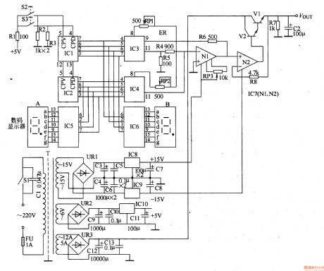
The numerical control D. C. regulated power supply circuit introduced in the example adopts LED to indicate output voltage's magnitude with features of visual display,convenient operation,high-precision voltage regulation.Its output voltage range is 0-9.9V and output current is 5A.
Circuit's Work principle
The numerical control D. C. regulated power supply circuit is composed of power regulation voltage circuit,operation and control circuit,display driver circuit,D/A converter circuit and regulated output circuit and it is showed as the picture 5-23.The power regulation voltage consists of mains switch,S,fuse,FU,mains transformer,T,rectifier bridge,UR1-UR3,capacitor,C1,C3-C13 and voltage regulation IC,IC8-IC10. (View)
View full Circuit Diagram | Comments | Reading(882)
TTL level / ± l2V level conversion circuit
Published:2011/7/6 4:59:00 Author:Lucas | Keyword: TTL level, ± l2V level , conversion circuit
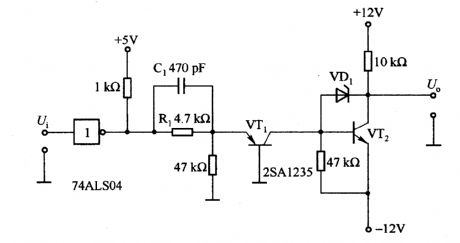
In the circuit, VTl is the switch circuit, of which base is grounded circuit. When 74LSO4 output is in high level, VTl is conducted, and its collector current changes into the base current of VT2, VT1 is also conducted, and the level with the output in U is changed into l2V to add with the collector saturation voltage of VT2. This circuit can not make high-speed switching work. If Rl is connected to capacitor Cl with capacity in several hundred pF in parallel, and the base - collector of VT2 is connected with the Schottky diode VD1, VT2 is conducted and not in the completely saturated state, so to some extent, it will increase the switching frequency.
(View)
View full Circuit Diagram | Comments | Reading(799)
Numerical Control D. C. Regulated Power Supply Fourteen
Published:2011/6/14 12:54:00 Author:Michel | Keyword: Numerical Control, D. C., Regulated Power Supply, Fourteen
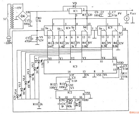
The numerical control D. C. power-supply circuits-fixed introduced in the example uses single button control means and its magnitude of output voltage are divided into six grades,namely,1.5 V,3V,5V,6V,9V and 12V.Its output power is 20W.Its femature is that open it after cutting off utility power and the output voltage is the lowest voltage,1.5V
Work's Principle of the Circuit
The numerical control D. C. power-supply circuits-fixed is composed of input constant voltage circuit,impulsator,control output or indication circuit and it is showed as the picture5-33.The input constant voltage circuit consists of ,switch,S1,mains transformer,T,rectifier bridge,UR,filter capacitor,C1,C2,current-limiting resistor,RO and voltage regulator diode,VS. (View)
View full Circuit Diagram | Comments | Reading(966)
Voltage / frequency conversion circuit composed of NE555
Published:2011/7/10 22:23:00 Author:Lucas | Keyword: Voltage conversion , frequency conversion
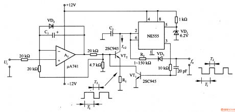
In the circuit, NE555's oscillation frequency is controlled by the VT2, and during its pin 3 in the low output waveform (output waveform of the T1 period), as VTI stops, VT2 is conduction with current Ic2 flowing, and the size is controlled by the output voltage of Al. C2 discharge time T1 = C2U2 / (2Ic2), in the formula, Uz is the stable voltage of VD1. NE555 output is in high level, the current flows VD3 by pin 3. R2 and C2 have current flowing. Then VTl is switched into saturated conduction, and the base of VT2 is equivalent to short-circuit, so VT2 ends, and the collector current Ic2 is zero.
(View)
View full Circuit Diagram | Comments | Reading(4345)
Load Power Adjustor One
Published:2011/6/14 12:50:00 Author:Michel | Keyword: Load Power Adjustor, One
The load power adjustor adopts zero passage adjusting power circuit and the circuit is simple but with good effect.Its dependability is also high and it can regulate kinds of heating appliances' power such as electric hair dryer, electric cooker,electric iron and series wound motor's speed.
Circuit's Work Principle
The bearing power adjustor circuit is composed of power supply circuit,zero passage test circuit and power regulation circuit and it is showed as the picture 5-54.The power supply consists of mains transformer,T,commutation diode,VD1 and VD2 and filter capacitor,C. (View)
View full Circuit Diagram | Comments | Reading(548)
12V,24V battery automatic charger circuit
Published:2011/7/8 3:22:00 Author:Fiona | Keyword: 12V,24V battery automatic charger
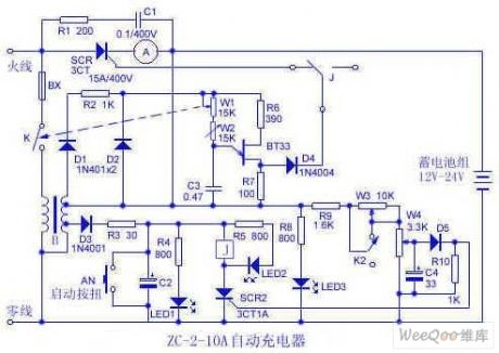
unijunction transistor BT33, C3, W1, W2 and other components form the relaxation oscillator.The pulse signal produced by he relaxation oscillator is transmited through isolation diode D4 to the control pole of thyristor SCR1 , adjusts the resistance of W1 to change the trigger the conduction angles of SCR1, which changed the charge current. Thyristor SCR2, relay J, W3, W4, D5 and other components form the storage battery in automatic protection circuit, when the battery voltage isfillingto the upper limit the W3, W4 set, D5 breakovers, SCR2 is triggered to breakover, LED2 display and relay picks, at the same time J switches to the normally open, cuts off SCR1 control pulses focused, that is to stop charging the battery. K2 is 12V, 24V battery charging switch, the icon places12V stalls.
(View)
View full Circuit Diagram | Comments | Reading(4854)
| Pages:1558/2234 At 2015411542154315441545154615471548154915501551155215531554155515561557155815591560Under 20 |
Circuit Categories
power supply circuit
Amplifier Circuit
Basic Circuit
LED and Light Circuit
Sensor Circuit
Signal Processing
Electrical Equipment Circuit
Control Circuit
Remote Control Circuit
A/D-D/A Converter Circuit
Audio Circuit
Measuring and Test Circuit
Communication Circuit
Computer-Related Circuit
555 Circuit
Automotive Circuit
Repairing Circuit