
Circuit Diagram
Index 1755
Frost Alarm (1)
Published:2011/5/16 3:13:00 Author:Sue | Keyword: Frost, Alarm
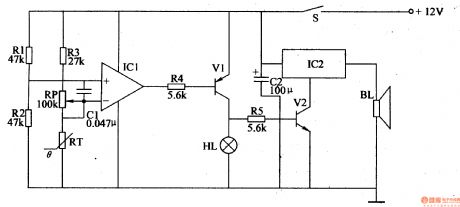
Working Principle:
When there is no frost, the temperature is relatively high, so RT's resistance value is low. IC's syntropy input terminal will have a higher voltage than its reverse input terminal. The output terminal will output high level, making V1 and V2 disconnected, HL is not illuminated. IC2 doesn't work and BL makes no sound.
When there is frost, the temperature becomes lower,so RT's resistance value will be higher, making IC's reverse input terminal have a higher voltage than its syntropy input terminal. The output will have low level, making V1 and V2 connected, and HL is illuminated. IC2 begins to work and BL makes a warning sound. (View)
View full Circuit Diagram | Comments | Reading(707)
Single-Phase Motor Controlled Circuit
Published:2011/5/16 3:12:00 Author:Sue | Keyword: Single-Phase, Motor, Controlled
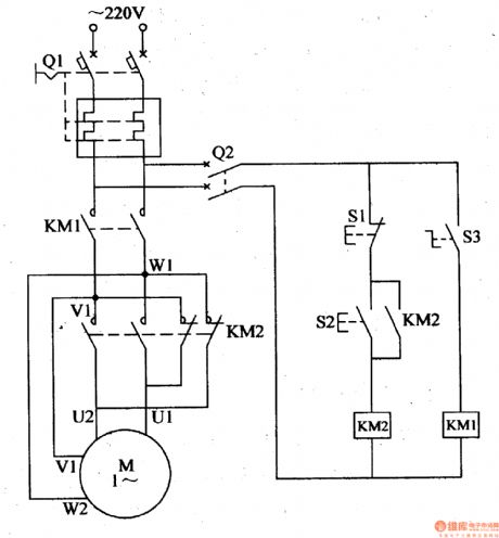
When Q1 and Q2 are connected, push the starting button S2. The 220V ac voltage will go to KM2, making KM2 connected, and the motor M will begin to work. When S2 is released, KM2 is still connected. When push S1, KM2 will be disconnected and M stops working.
When S3 is connected, KM2 will be connected and M will rotate in a reverse direction.
When there is too much voltage and current on M, Q1 will be disconnected automatically to protect M. If KM1 or KM2's coils are short, Q2 will be disconnected automatically. (View)
View full Circuit Diagram | Comments | Reading(6082)
Double MOS Memory Interface Circuit
Published:2011/5/18 9:43:00 Author:Joyce | Keyword: Double MOS, Memory , Interface
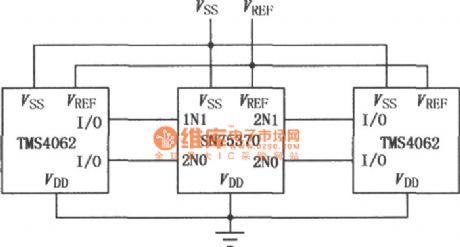
SN75370 is a monolithic integrated read/write interface circuit, which can be used as input/output interface in 4062 and in MOS RAM and TTL circuit of the same type. It can be connected directly with I/O interface of similar MOS RAM like 4062 . When it is written into operation, the drive can provide a complementary high voltage output with a high sensitive read operation.TTL will input with compatible diode clamp of DTL,and output with compatible data of DTL .The output endof data can act as AND connection. And the power supply has a extensive range. As shown in the figure is the interconnection graph of SN75370 and 4062. (View)
View full Circuit Diagram | Comments | Reading(639)
Meeting Timer Circuit
Published:2011/5/18 9:39:00 Author:Joyce | Keyword: Meeting, Timer
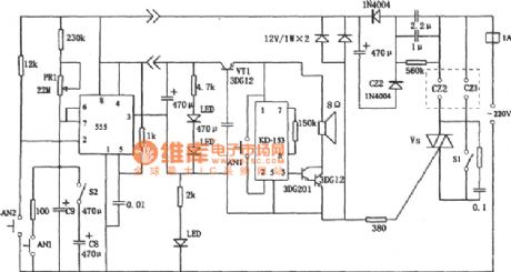
As shown in the figure the limited time of this circuit ranges from 5 minutes to 1 hour. PR1, C8 and C9 are the timing components. The sockets for 220V AC power supply,which controls the audio power amplifiers are CZ1 and CZ2. To press AN2, 555 means reset and start .Its feet ③ outputs high level, which will trigger the thyristor to make it breakover.And when CZ1 and CZ2 have voltage,the timing will begin. KD - 153 will produce sounds for a few seconds to indicate the circuit is proper.When the timer stops,feet 5553 will output low level,thus VS will turn off, and no voltage will be on CZ1 and CZ2.After hearing sounds produced by KD - 153 for a few seconds ,the limited time for the meeting is up.
The circuit is alsoapplicable for other control circuits which needs timing. (View)
View full Circuit Diagram | Comments | Reading(581)
Constant Current Supply Circuit with Operational Amplifier
Published:2011/5/18 9:42:00 Author:Joyce | Keyword: Constant Current , Supply , with Operational Amplifier
View full Circuit Diagram | Comments | Reading(628)
TV Signal Transformation Amplifier Circuit
Published:2011/5/18 9:41:00 Author:Joyce | Keyword: TV Signal, Transformation, Amplifier
As shown in the figure is a circuit used to transform and amplify all kinds of TV video signals output by various equipment,such as VCR, DVD players with weak output signals to be amplified.It can send the open circuit with radio-frequency signals to an extent with 7m-radius to make it possible for several TV to function at the same time. (View)
View full Circuit Diagram | Comments | Reading(758)
M494 (TV)infrared remote control receiving microprocessor
Published:2011/6/1 9:38:00 Author:Lena | Keyword: infrared, remote control, receiving, microprocessor
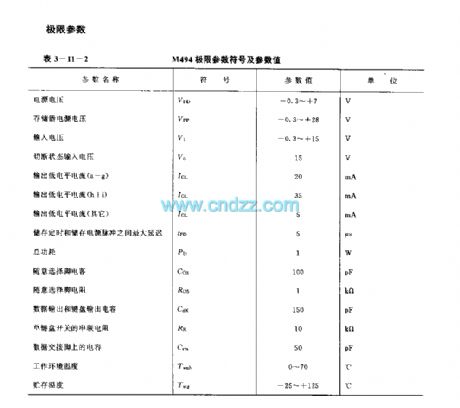
M494 is an infrared remote control receiving microprocessorappliedto TV etc.The related types are M708 and TDA2320.Package form is a 40-pin dual-in-line plastic package.
Functions:
*Minimum radius of input signal from remote signal input end(35th pin) is 0.5V(peak-to-pwak value),minimum pulse width is 8μs.
*Row(a-g) and line(D0-D4) form a 5×4 keyboard matrix,every key usesresistant(maximum value is 10KΩ)connecting rows and lines.
*The circuitcan prevent bounce.That is when a key closing more than 40ms,relevant instruction can be received;the key related to
boot-strap/standby,boot-strap/shutdown instructions,must close more than 100ms, the instruction can be received.
*Different states obtainedthrough function select end (6th pin) and keyboard line(D0-D4) whether or notconnecting a diode,to select function.
(View)
View full Circuit Diagram | Comments | Reading(561)
Video Enhancement Circuit
Published:2011/6/6 0:23:00 Author:Joyce | Keyword: Video, Enhancement
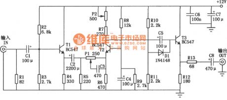
The video enhancement circuit shown in the graph can increase the high frequency component of video signals,thus enhancing the contrast of the televison image. It can be connected between the output end of VCR and the input end of television SCART. The transistorT1 in the circuit acts as a buffer. Resistance Rl guarantees that the input impedance of this circuit is about 75 Ω. Signals will be applied to the enlarger T2,and their gains depend on the position of the potentiometer P2. The frequency characteristics of T2 base signals are restricted by P1, R6, C6 ,so in a certain extent it can be controlled by the users (through P1). Buffer stage T3 provides enough electricity to drive most 75 Ω loads correctly .Adjusting potentiometer P2 can set the output to be 1Vp - p (electric level should be 2Vp - p for output to open circuit). (View)
View full Circuit Diagram | Comments | Reading(745)
Simulation Karaoke Accompaniment Amplifier Circuit
Published:2011/6/6 0:24:00 Author:Joyce | Keyword: Simulation , Karaoke Accompaniment , Amplifier
As shown in the figure is the simulation karaoke accompaniment amplifier circuit. According to the features of audiotapes, this circuit can remove the same part in the left and right channel of the stereo and leave the accompanying music . (View)
View full Circuit Diagram | Comments | Reading(3401)
Double T Sinusoidal Oscillator with Stable Output Circuit Composed of LM170
Published:2011/5/25 4:05:00 Author:Joyce | Keyword: Double T, Sinusoidal Oscillator, Stable Output, LM170
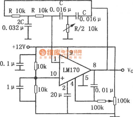
As shown in the figureis the circuit for double T sinusoidal oscillator with stable output.This circuit uses automatic gain control amplifier LM170 to stabilise its amplitude . In this way, the wave form would have no distortion. Even when the double T circuit and amplifier have changes, the output amplitude can remain constant.Using the component values in the graph can compensate the change of 40dB. 100k potentiometer is used to change the threshold level controlled by automatic gain to change the output level. The oscillation frequency of circuit is:F0 = 1/2 PI RC
If using the component values in the figure, the oscillation frequency is about 1kHz. (View)
View full Circuit Diagram | Comments | Reading(987)
4-hour AC Power Supply Timer Circuit
Published:2011/5/18 9:39:00 Author:Joyce | Keyword: 4-hour, AC Power Supply , Timer

As shown in the figure is a 4-hour AC power supply timer circuit. In this circuit, BH4024 is a 7-level binary system counter/frequency divider, and 555 is a timebase circuit. AN is a timing touch button. Everytime you press AN once, it could output four-hour 220V AC power supply, after 4 hours,it will outage. This circuit can be used in working time whose morning and afternoon is separated by4-hour as an unit.
(View)
View full Circuit Diagram | Comments | Reading(2017)
Simple Sine Wave Generator Circuit Composed of μA741
Published:2011/5/25 4:04:00 Author:Joyce | Keyword: Simple, Sine Wave, Generator, Composed of μA741
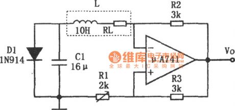

(View)
View full Circuit Diagram | Comments | Reading(637)
Stable Sinusoidal Oscillator Circuit Composed of F007
Published:2011/5/25 4:05:00 Author:Joyce | Keyword: Stable , Sinusoidal Oscillator , F007
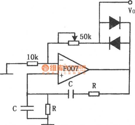
As shown in the figure is a stable sinusoidal oscillator circuit. In order to get a stable oscillation, the gain of the circuit should be 1. If the gain is too large, there will be distortion of the waveform; If gain is too small, the vibration may stop . This circuit uses two diodes to stabilize the oscillations. When the output voltage is too low, the diode will close, and the negative feedback will be cut off. Then the loop gain and the output voltage will increase.When the output goes up to a certain value, the diode will conduct, and the loop gain andoutput voltage will decrease. Repeatedly,the output amplitude will be kept in a certain value. The potentiometer in the figure is to regulate the output amplitude and the degree of distortion. The oscillation frequency of the circuit is determined by resistance R and capacitance C , the formula being :
F0 = 1/2π RC. (View)
View full Circuit Diagram | Comments | Reading(753)
Sinusoid Generator Circuit Composed of Inverter
Published:2011/5/25 4:06:00 Author:Joyce | Keyword: Sinusoid Generator, Inverter
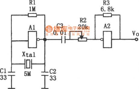
As shown in the figure is a sinusoid generator circuit composed of inverter.This circuit can get high stable sine waves above several MHZ. A1 and crystal oscillator in the figure consist a oscillating circuit . The output of A1 will export sine wave signals after passing through buffer A2. In the circuit, A1 is a linear amplifier,and the whole circuit work in a state of amplification. Due to the different characteristics of the crystal oscillators being used, output frequency and voltage of the circuit are different. R2 can be used to adjust waveform. In order to obtain accurate oscillation frequency,you can have a fine adjustment by connecting semi-variable capacitors in parallel between the ends of capacitance C1 . The oscillation frequency of circuit is determined by crystal oscillators. Change of crystal oscillators will bring out alterations in output signal frequency. (View)
View full Circuit Diagram | Comments | Reading(643)
Can be linear output 10MV / ° C voltage IC temperature conversion circuit
Published:2011/6/2 4:26:00 Author:Fiona | Keyword: linear output, temperature conversion
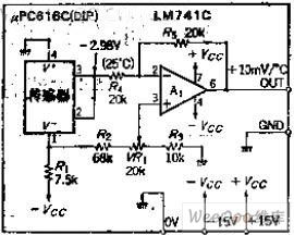
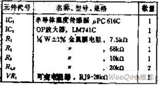
Circuit Work
The IC internal temperature sensor can obtain the voltage output which is proportional with 10MV/°K.The lead 2,3 of the internal amplifier play the role of buffer after connectings.It can make the output voltage is zero power at any temperature whenusing the level shift circuit A1.The lead 1,4 of the sensor internal have 6.85V zener diode ,obtain 1MA ~ 5MA home bias current from R1.Reference voltage inputs from the R2, which is obtained by variable resistor VR1 partial pressure.
(View)
View full Circuit Diagram | Comments | Reading(865)
Voltage Controlled Sinusoidal Sscillator Circuit Composed of MC1046B
Published:2011/5/25 4:07:00 Author:Joyce | Keyword: Voltage Controlled , Sinusoidal Sscillator, MC1046B
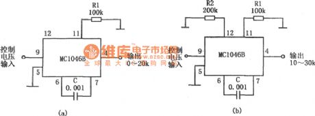
As shown in the figure ab is the voltage controlled sinusoidal oscillator circuit composed of MC1046B . When the control input voltage is 0 ~ 5V, the output can be sine wave signals with a frequency of 0 ~ 20kHz. The frequency range is determined by resistance R1 and capacitance C, so changes in resistance and capacitance can bring about alteration in oscillation frequency. If you connect resistance R2 outside the feet12 ,you can change the oscillation frequency range. If R2 = 2R1, then the oscillation frequency will be 10 ~ 30kHz. (View)
View full Circuit Diagram | Comments | Reading(610)
Broad-band Sine Wave Voltage-controlled Oscillator Circuit Composed of LF356N
Published:2011/6/6 0:21:00 Author:Joyce | Keyword: Broad-band , Sine Wave , Voltage-controlled Oscillator
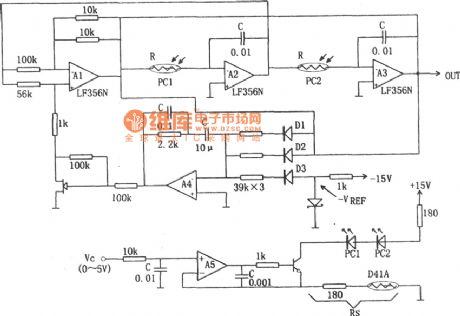
As shown in the figure is the broad-band sine wave voltage-controlled oscillator circuit. The oscillation frequency of the circuit depends on integration resistor R and capacitance C. The oscillator constitutes of resistance R controlled by an external voltage VC. The variable resistance in the circuit uses optical coupler PC1 and PC2, and the rectification circuit is detected by average value. The actual operating frequency of the circuit is above dozens of Hertz. In addition, the characteristics of control voltage VC depends on the characteristics of the photoelectric coupler used (View)
View full Circuit Diagram | Comments | Reading(1323)
Circuit of Sine wave Oscillator with Ajustable Frequency and Constant Amplitude
Published:2011/5/25 4:25:00 Author:Joyce | Keyword: Sine wave, Oscillator , Ajustable Frequency, Constant Amplitude
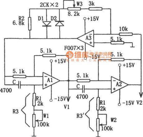

As shown in the figure is the circuit of sine wave oscillator with ajustable frequency and constant amplitude. This circuit constitutes of a two-stage phase-shifting circuit and a one-stage linear inverting amplifier, which are connected in series. And the phase-shifting circuit is composed of integrated operational amplifier A1, A2 and RC. Because the phase shift of inverter A3 is 180o, the two-stage phase-shifting circuit should also have a phase shift of 180o to ensure that it can meet the overall phase shift of 360o required by the oscillation. The dynamic resistances of diode D1, D2 are quite large when the voltage is low, so the gain of the inverting circuit composed of As is high to make sure the starting of oscillation of the circuit. Oscillation frequency of the circuit is: (View)
View full Circuit Diagram | Comments | Reading(665)
infrared modulation detection circuit diagram
Published:2011/5/11 1:46:00 Author: | Keyword: infrared, modulation, detection
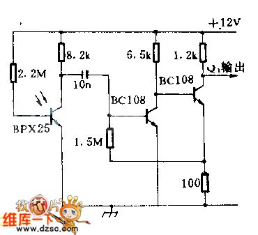
When a 1lx peak value light signal isinputted in the photoelectric cell,then the signalgo through bipolar amplifier,will output 400mV peak value;the detector sensitivity at 4KHZ is lower 3dB than at 1KHZ;when using F:2 calibration ten or parabola reflector on the infrared signal source and detector,the detect distant can be 30.48m(100 feet).This circuit can be used in high secrecy communication system.
(View)
View full Circuit Diagram | Comments | Reading(763)
put 4 ~ 20MA into the positive and negative 10 V current-voltage conversion circuit
Published:2011/5/11 21:53:00 Author:Fiona | Keyword: current-voltage conversion
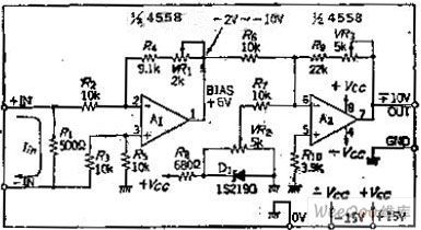
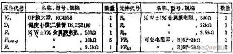
Circuit Work
The purpose of using OP amplifier A1 is to consider that if the one end of sensor resistance R1 can not be grounded, R1 can be used as a differential amplifier. However, if the resistance R6 and R7 of the summation meter have high value,you can remove A1. In order to make A3 output -10V when the current is 4MA, the A1 should be made output in -2 ~-10V.
OP amplifier A2 is the summing amplifier putting unipolar input into bipolar output. In order to output 0 when the current is 12MA, add the polar opposite +6 V for subtraction. VR3 is used to determine the slope. Because it should enlarge 8V which is input to 20V, so the magnification should be A = 20 / 8 = 2.5 times. (View)
View full Circuit Diagram | Comments | Reading(2488)
| Pages:1755/2234 At 2017411742174317441745174617471748174917501751175217531754175517561757175817591760Under 20 |
Circuit Categories
power supply circuit
Amplifier Circuit
Basic Circuit
LED and Light Circuit
Sensor Circuit
Signal Processing
Electrical Equipment Circuit
Control Circuit
Remote Control Circuit
A/D-D/A Converter Circuit
Audio Circuit
Measuring and Test Circuit
Communication Circuit
Computer-Related Circuit
555 Circuit
Automotive Circuit
Repairing Circuit