
Circuit Diagram
Index 1760
100-nary counter circuit
Published:2011/6/9 21:19:00 Author:John | Keyword: 100-nary counter

Define the level of integration counter. 1 # chip is low (equivalent to one bit) and 2 # chip is high (the equivalent of ten). Start counting from the low bit and send the counting pulse CP into 1# (low) the CP terminal of integrated counter.
B. Look for carrying signal. It is delivered from the injection terminal C. This is the process for counting from 0 to 9. When Q3Q2Q1Q0 reaches 1001(9), high signal has been delivered. C. 74LS160 is the most effective integration counter for the CP’s rising edge. And the chip at high height requires a high level trigger with rising edge pulse in order to count triggering number. (View)
View full Circuit Diagram | Comments | Reading(530)
The OTL Earphone Amplifier composed of double triode ECC822 electronic value circuit diagram
Published:2011/6/2 21:11:00 Author:Sophia | Keyword: Double triode, ECC822electronic value, OTL Earphone Amplifier
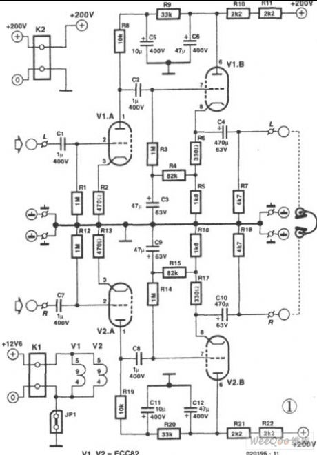
As shown, the curcuit is using the double triode equivalent of E802C、E82CC and North American12AU7 and domestic 6N10as amplifier, This kind of transistor is characterized by excellent indicator and long service life. HD head Amplifier will produce enough signal amplitude to drive earphone. Audions of base pin 1,2,3 amplify signal. Input signal arrives circuit board through 50kΩvolume control logarithmic potentiometer p1(p1 is not shown in the diagram), and pass C1、R1 to input to pre-amplification. meanwhile,R1、C1l must provide indispensible negative grid bias. Gain is decided by R8, and maximum input voltage is determined by R2. R9 is to determine that static anode current is in utmost linear part of characteristic curve. The input signal amplified by phase reversal in positive pole arrives the second stage grid through C2 coupling.The second stage cathode resistance is divided to R5 and R6. R5 and R6 connect in series to form load resistance.
(View)
View full Circuit Diagram | Comments | Reading(810)
The high voltage input FET power amplifier circuit diagram
Published:2011/6/10 22:01:00 Author:leo | Keyword: The high voltage input FET power amplifier circuit diagram, 2SA639, 2SC1279, 2SA818, 2SA633, 2SC1628
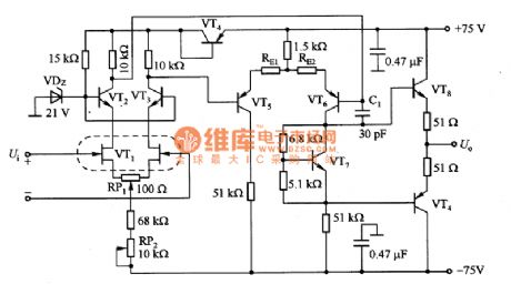
As the picture 1 shows, it is a high voltage input power amplifier circuit. The input VT1 of the circuit adopts FET tube. And its drain is connected to common base amplifier formed by VT2 and VT3, which is used to electric level move in order to prevent high voltage from being connecting to the drain of VT1. VT5 and VT6 are differential amplifying circuit.When the emitter is connect is added the current feedback, convert rate will be improved. Feedback resistance value of RE1 and RE2 need to be 0 to 5OOΩ. VT4 should be connected to be a diode which is used to make up the difference of UBE of VT5 and VT^ causing by temperature changes. VT8 and VT9 are push-pull output circuit. (View)
View full Circuit Diagram | Comments | Reading(4662)
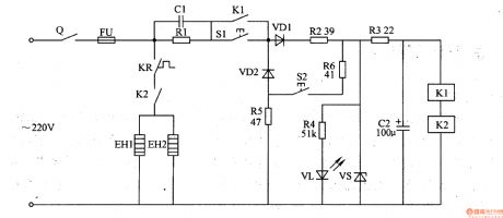
Electronic Sterilizer (the 2nd)
Published:2011/5/19 8:23:00 Author:Felicity | Keyword: Electronic Sterilizer (the 2nd),
Work of the circuit
The electronic sterilizer circuit consists of power circuit, control circuit and heating circuit. (It is showed in picture 9-97).Turn on Q’s control derail and press button SI. 220V AC voltage is bucked, rectified, limited and stabilized by CI, VDI, R2, VS. Then the voltage separates into two parts. One lightens VL after being bucked and limited by R4 while the other one supplies the working voltage to K1 and K2 after being bucked and limited by R3 and filtered by C2. (View)
View full Circuit Diagram | Comments | Reading(592)
Disinfectant Manufacturer (the 2nd)
Published:2011/5/19 21:12:00 Author:Felicity | Keyword: Disinfectant Manufacturer (the 2nd),
Work of the circuit
The disinfectant manufacturer circuit consists of power changing circuit, pilot light controlling circuit, electrode driving circuit and timer circuit. (Iit is showed in picture 9-93.).
Put 500ml salting liquor in the cup of Disinfectant Manufacturer and turn on the power. 220V AC voltage produced +6V voltage after being reduced rectified and filtered. The voltage separates into two parts. One of them supplies pole and its driving circuit while the other one supplies to timing circuit, pilot light controlling circuit and pole driving circuit. Here diode VLI starts to work which implies the beginning of work. When the timer has worked for about 60min diode VLI becomes dark which implies that the disinfectant has been done. (View)
View full Circuit Diagram | Comments | Reading(493)
Patient SOS Appliance Two
Published:2011/6/6 9:29:00 Author:Felicity | Keyword: Patient SOS Appliance,
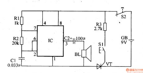
This patient SOS appliance consists of trigger circuit and oscillator. After the patient press S1, +9V voltage put on the gate pole of VT through S2, R3 and S1 to trigger VT on, and the oscillator is on and at work. The oscillator signal at the frequency about 1 KHz is output by pin 3 of IC to drive speaker BL send out a high frequency alarm sound. After the medicine box is open, S1 is off and VT cut off, then oscillator is power off and BL stops. (View)
View full Circuit Diagram | Comments | Reading(586)
Burr-Brown 3652 Isolation Amplifier Circuit
Published:2011/6/2 10:13:00 Author:Joyce | Keyword: Burr-Brown 3652, Isolation, Amplifier
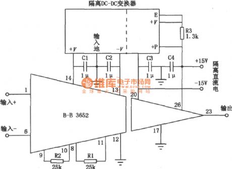
As shown in the figure is a circuit mainly composed of Burr-Brown 3652 isolation amplifier? Both isolated and insolated parts of 3652 are supplied by special power source 722,which generates two independent power supplies of ±15V , each being isolated with 50/60Hz ac power supply. And power source 722 itself is provided with ± 12V ac power supply. In some circumstances, the insolated part (which is connected with the output end) is supplied with bipolar dc power supply of 50/60Hz ac power supply, such as± 12V or±l5V power supply. But in no case would the isolated dc power be supplied with ac power. (View)
View full Circuit Diagram | Comments | Reading(754)
1kHz Sinusoidal Oscillator Circuit
Published:2011/5/29 0:59:00 Author:Joyce | Keyword: 1kHz , Sinusoidal Oscillator
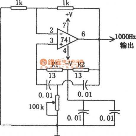
As shown in the figure is the 1 kHz sinusoidal oscillator circuit. This circuit would generate 1000Hz sine wave through an ordinary operational amplifier 741 on the basis of double T circuit. To adjust the 100kΩ potentiometer will make the circuit start oscillation, and the oscillation frequency is determined by R1 and R2,which are equal in value generally. The oscillation frequency is inversely proportional to the resistance value. Usually the range of resistance is 4.7 ~ 18 Ω , and when the value of R1 and R2 is set, the required capacitance can be determined. In the above figure, the value of the resistance is 13Ω,and the capacitance is 0.01 / u F and the oscillation frequency is 1kHz. (View)
View full Circuit Diagram | Comments | Reading(2253)
Automatic Timing Controller Circuit Composed of 555
Published:2011/5/29 1:19:00 Author:Joyce | Keyword: Automatic, Timing Controller, 555
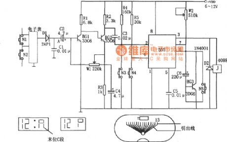
As shown in the figure is the automatic timing controller circuit. This circuit constitutes of an electronic watch, detection circuit (C1, D1), amplifying circuit, monostable multiply delay circuits (555, BG3 W2, C6 and), and relay J etc.
And the timing signal source is from the end part of the electronic watch segment C. When the end part P changes into R,the voltage of segment C will rise to 3V.And the signal will be detected D1、C1 and amplified by BG1 and BG2 before it is sent to feet ② of 555 to trigger the operation of 555 circuit. When the negative pulse of BG2 comes, the monostable multiply delay circuit would turn, then feet ③ would output high level, and the time of monostability will be 1.1Rw2C6β,βbeing the amplification factor of the current of BG3. (View)
View full Circuit Diagram | Comments | Reading(564)
Automatic Controller Circuit of Amplification and Exposure Time
Published:2011/5/29 1:35:00 Author:Joyce | Keyword: Automatic Controller, Amplification , Exposure , Time
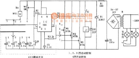
As shown in the figure is the automatic control circuit of amplification and exposure time . This circuit constitutes of step-down and rectifier circuit, monostable timing circuit and relay control circuit etc.The monostable timing circuit is composed of IC (555)、photosensitive detection head R0,and capacitance C1 ~ C4 etc. The length of timing depends on the time constant of the charging and discharging circuit.R0 is the photoconductive resistance. To stir the switch K2 will have four speed gears of exposure mode, 1, 2, 3 are automatic control, whose possess 3 kinds of exposure:” bright , normal and dark ,while 4 presents manual control. (View)
View full Circuit Diagram | Comments | Reading(532)
Automatic Timing Intermit Irrigation Control Circular Composed of 555
Published:2011/6/2 2:56:00 Author:Joyce | Keyword: Automatic , Timing, Intermit Irrigation , Control , 555
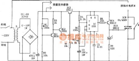
As shown in the figure is an automatic timing intermit irrigation control circuit. This circuit constitutes of a step-down rectifier circuit, an on-off control circuit, harmonic oscillators (R5, R6, 555, W2, C2) and bidirectional triode thyristor SCR control circuit etc.
The humidity sensors need to be connected into the circuit can be two graphite rods with brass caps on both ends. When the soil is dry, the electric conductivity between the two graphite rods is low, so the resistance is large. After differential pressure, BG1 will cut off while BG3 and BG2 will conduct. When the soil is moist, the resistance between the two graphite rods is small, thus BG1will conduct, and BG2, BG3 will cut off .The harmonic oscillators will stop in absence of power supply, and make tube BG4 and SCR cut off. Therefore, the corresponding pumping motor will not work. (View)
View full Circuit Diagram | Comments | Reading(1433)
Class Bell Automatic Controller Circuit Composed of 555
Published:2011/6/2 3:14:00 Author:Joyce | Keyword: Class Bell , Automatic , Controller, 555
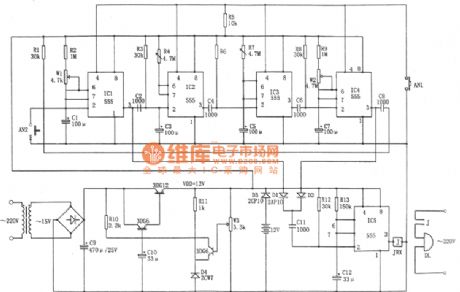
As shown in the figure is a class bell automatic controller circuit. It includes a step-down rectifier circuit, a circular program timing circuit, and an executive control circuit etc. IC4~ IC1 are trigger delay circuit, and the delay time can be adjusted by regulating charge-discharge time RC. IC5 is ringing time timing control circuit, and the delay time td5 is 1.1 R13C12. The output of IC4 IC1 in the circular program timing circuit is sent to D1, D2, then goes through capacitor C11 to trigger IC5 to output high level (feet③),which would make the relay actuate, thus supply the bell DLwith power.
(View)
View full Circuit Diagram | Comments | Reading(696)
Low-power liquid crystal display 3 1/2 A-D converter circuit
Published:2011/6/3 20:53:00 Author:Fiona | Keyword: Low-power liquid crystal display
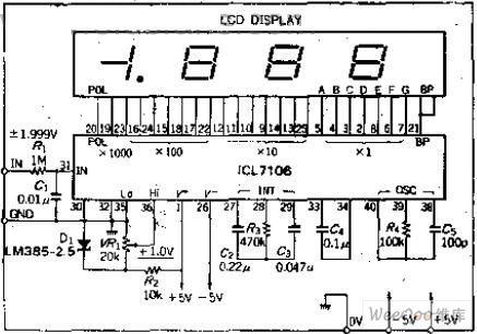
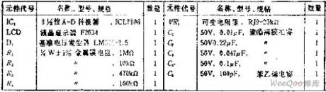
Circuit function
This is a digital display type A-D converter.It is suitable for portable small measuring instrument. Because of the use of liquid crystal display andLow consumption, Full range display voltage is 1.999V. If the input voltage is greater than this value, it should be added a attenuator.The circuit is more used for measuring instrument.Its power source voltage is in positive and negative 5V.
Circuit Work
3 1 / 2-bit A-D converter ICL7106 is a monolithic LSI that can directly drive liquid crystal display, is general Instrument IC and other companies have processed products. A - D convert way is ordinary double integral type, differential input circuit can input positive and negative about 1V phase voltage, the internal does automatic zero set. Circuit adjustment can only use VR1.
(View)
View full Circuit Diagram | Comments | Reading(2473)
Widely used IC monolithic multiplication circuit
Published:2011/5/11 5:49:00 Author:Fiona | Keyword: IC monolithic multiplication
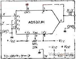

Circuit functionIn addition to be general multiplication, Analog multiplication has many other uses, such as balanced modem, synchronous detection, voltage controlled attenuator, oscillators. This circuit is a basic wiring diagram of an analog device company’s single IC multiplier AD532. Because it has been minute adjusted by the laser in-house, it can remove potentiometer that being used to adjust the X, Y input set of partial balance, just adjusts the output as long as the home side.
Circuit WorkAD532 is a differential input of the four-quadrant multiplier. It can be EO = [(X1-X2) * (Y1-Y2)] / 10 op. The input voltage range is 0 ~ +10 V, usually uses 1 / 10 scale factor.IC internal is multiplication unit composed of multiplier circuits known as Gilbert , the output impedance is low and no needs external components. The internal IC has been minute adjusted by the laser, there is no need cumbersome adjustment.The circuit only has the output offset adjustment V.AdjustmentBecause the circuit only has the offset adjustment, it only illustrates the AD533 that has not be minute adjusted.In Figure A just has one more variable resistor.It can use the basically same adjustment with the AD532.
(View)
View full Circuit Diagram | Comments | Reading(1019)
the isolated current - frequency conversion circuit to convert 4~20MA to 10KHZ
Published:2011/5/11 7:15:00 Author:Fiona | Keyword: the isolated current - frequency conversion, convert 4~20MA to 10KHZ,
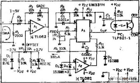
Circuit Work
This circuit consists of two parts, namely, converting current - voltage section and the use of VF converting voltage into frequency by VF converter section.The current - voltage converter uses a 250Ω resistor R1, produces the voltage at R1's both ends, and then uses OP amplifier 1 to turn the voltage into 0 ~-10V, so the reverse magnification should be 2.5 times.
When current is 4MA, in order to make the output of A1 is 0, it must use home bias circuit. It can add the voltage at inverting input to form the home bias. If don't use the method of the home bias,put the in-phase input to ground. It also can be converted to 2 ~ 10KHZ frequency output when A1 magnification is 2.
V-F Converter uses NS company's LM331, its detailed structure has been introduced in the company's products' manuals .In order to improve linearity, add the OP amplifier A2, which is the current input type, full range is 0 ~ 100UA, therefore,according to the input voltage range, R5's resistance should be 100K, in the feedback loop, C2's role is to maintain Loop stability, the capacity is selected by range of the input signal.
(View)
View full Circuit Diagram | Comments | Reading(1766)
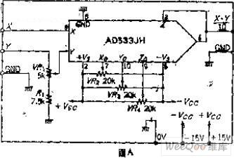
achieving multiply the analog input and digital data R.SINθ conversion circuit
Published:2011/5/12 5:06:00 Author:Fiona | Keyword: achieving multiply the analog input and digital data, R.SINθ conversion
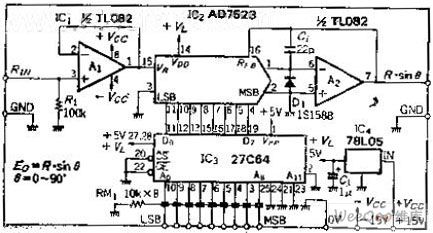
Circuit function
he circuit outputs Y (Y = R. SINθ) function (in Figure A,X, Y is as coordinates, R is representative of the analog input, Y is representative of the function output),θ's selected range is 0 to 90 degrees.90 to 180 degrees and 0 to 90 happens is reciprocal.To make the data can wait until 180 degrees, the control signal uses two BCD code +1 data bits.
Circuit Work
This is an analog input and digital data multiplication circuit which does the R computing and the digital data values is from 0 to 255.In advance, make the ROM data corresponding to the sine function good,because AD7523 is a positive logic input,SIN0 degree = 0, D = 00; SIN90 degree = 1, D = FFH (255/255 ≈ 1).Calculate SIN0 ~ 90 degrees to a degree level,then multiply by 25and switch to binary data to store in the P-ROM.
(View)
View full Circuit Diagram | Comments | Reading(766)
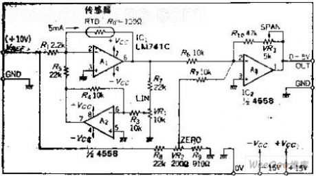
simplified resistance temperature circuit that improving the linear by using positive feedback
Published:2011/5/13 2:57:00 Author:Fiona | Keyword: improving the linear by using positive feedback

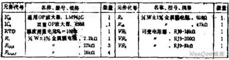
Circuit function
This circuit is a temperature measurement which uses a positive feedback way and has a linearizer,if temperature rises, the current flows through RTD will increase,if the temperature range is 0 ~ 500 ° C, we can obtain 0 ~ 5V of Voltage output, the error can be controlled within plus or minus 0.08%. Circuit Work OP amplifier A1is the inverting amplifier, it connects with RTD in the feedback loop, when set side the constant current with 5MA currents, A1 output may have-0.5V voltage. Assume that the RTD's variation is △ R,the output voltage's variation is △ R * 5MA. (View)
View full Circuit Diagram | Comments | Reading(727)
the constant voltage-driven bridge sensor circuit constituted by OP amplifier feedback loop
Published:2011/5/13 3:19:00 Author:Fiona | Keyword: constituted by OP amplifier feedback loop, the constant voltage-driven
Circuit function
This is a drive, detection circuit that is suitable for use bridge sensors.It is Driven by constant voltage, the voltage is ± 2.5V, if necessary to use the IC generating reference voltage,it can also use ± 5V or ± 10V.
Circuit Work
OP amplifier A1 is a +2.5 V reference voltage generating circuit, in order to output ten mA current, adds the current enhancer TT1. If the resistance of the bridge sensor is equivalent, A2's inverting input is hypothetical, so TT2 emitter voltage should be -2.5V.
(View)
View full Circuit Diagram | Comments | Reading(1121)
Numerical Control D. C. Regulated Power Supply Three
Published:2011/6/2 10:57:00 Author:Michel | Keyword: Numerical Control, D. C. , Regulated Power Supply, Three
The numerical control D. C. power-supply circuits-fixedintroduced in the example uses dallastat and three-terminal tunable voltage regulatoion IC to regulate the voltage and adopts LED,voltmeter to indicate voltage.
Circuit's Work Principle
The numerical control D. C. regulated power supply circuit is composed of power converting circuit,+5V voltage regulation circuit,voltage regulation control output circuit and LED indication circuit and it is showed as the picture 5-22.The power converting circuit consists of mains transfomer,T,rectifier bridge,UR and filter capacitor,CO.The +5V voltage regulation circuit is composed of resistor,R1,capacitor,C1 and C2 and three-terminal voltage regulation IC,IC5.
(View)
View full Circuit Diagram | Comments | Reading(829)
Numerical Control D. C. Regulated Power Supply Two
Published:2011/6/2 10:54:00 Author:Michel | Keyword: Numerical Control D. C. Regulated Power Supply, Two
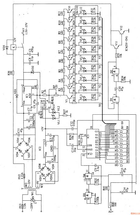
The numerical control D. C. regulated power supply circuit introduced in the example is controlled by tuch-button and digital integrated circuit.Its output voltage range is 1.5-37V divided into low voltage(1.5-15V) and high voltage(16.5-37V).
Circuit's Work PrincilpeThis circuit i scomposed of power supply input converting circuit,+5V voltage regulation circuit,functional mode indicating circuit and control circuit and it is showed as the picture 5-21.The power supply input converting circuit consists of fuse,FU1 and FU2,piezoresistor,RV,mains transformer,T and commutation diode,VD4-VD11.The +5V voltage regulation circuit is composed of filter capacitor,C4 and C5 and three-terminal voltage regulation IC,IC2.
(View)
View full Circuit Diagram | Comments | Reading(2777)
| Pages:1760/2234 At 2017411742174317441745174617471748174917501751175217531754175517561757175817591760Under 20 |
Circuit Categories
power supply circuit
Amplifier Circuit
Basic Circuit
LED and Light Circuit
Sensor Circuit
Signal Processing
Electrical Equipment Circuit
Control Circuit
Remote Control Circuit
A/D-D/A Converter Circuit
Audio Circuit
Measuring and Test Circuit
Communication Circuit
Computer-Related Circuit
555 Circuit
Automotive Circuit
Repairing Circuit