
Circuit Diagram
Index 251
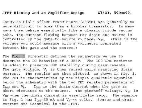
JFET BIASING TUTORIAL
Published:2012/12/6 19:56:00 Author:muriel | Keyword: JFET
View full Circuit Diagram | Comments | Reading(853)
Voltage Variable Capacitance (VVC) Diodes
Published:2012/12/6 19:54:00 Author:muriel | Keyword: Voltage Variable Capacitance (VVC), Diodes
View full Circuit Diagram | Comments | Reading(1100)
Silicon and Zener Diodes
Published:2012/12/6 19:54:00 Author:muriel | Keyword: Silicon and Zener Diodes
Silicon diodes are widely available and inhabit almost every junk box. I have tried using many types of diodes as voltage variable capacitors, but some types, such as rectifier diodes have a better range of variable capacitance than others. As stated before, reversed-biased diodes will decrease in capacitance as the voltage applied to them is increased. Do not expect the Q and thus the stability of a tuned circuit using silicon diodes to be that of better VVC diodes in a similar circuit. One particularly practical example of an application for using silicon diodes is for BFOs. In a BFO, there is typically a crystal and the desired frequency change is relatively small making silicon diodes attractive as the tuning device.
Earlier, I referred to W6WTUs HAM Radio Magazine article. From my own experiments, I confirmed Hugh's readings and found that rectifier diodes, are probably the most practical and easy silicon diodes to use as voltage variable capacitors. As far as rectifiers diodes go, the 1N4001 is probably the most commonly used in this application and a web search of HAM Radio electronic sites found its use in three different oscillator projects. From my experiment, the 1N4001 may exhibit a capacitance swing from 35 pF to 4 pF with a corresponding minimum and maximum reverse DC voltage of 0.5 and 12.0 volts. If you increase the voltage above 12.0, a lower capacitance may be realized but its significance is limited as it is getting into the non-linear area of the voltage versus capacitance curve and above normal QRP operating voltages. In addition, the linearity of the change in capacitance versus reverse voltage change is quite poor under ~5 volts for the 1N4001. I plotted the response curve for the 1N4001 and the results indicated that the best control voltage range to use for VFO tuning linearity is 5.0 to 12.0 volts. (View)
View full Circuit Diagram | Comments | Reading(925)
Bipolar Junction Transistors 2
Published:2012/12/6 19:52:00 Author:muriel | Keyword: Bipolar Junction Transistors
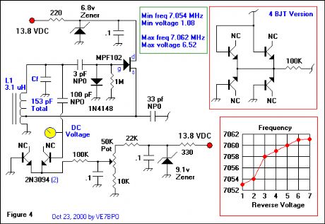
Experiments were conducted on this circuit and the minimum and maximum frequency and corresponding measured DC voltage on the BJT emitters for each was recorded. In Figure 4 as shown, the lower frequency/DC voltage was 7.054 MHz and 1.08 volts and the upper frequency/voltage was 7.062 MHz and 6.52 volts.
In the red insets are a schematic showing a four BJT version of this circuit and a plot of the reverse voltage versus frequency of the Figure 4 VFO without the series 22K and grounding 10K resistor ( This accounts for the frequency differences between the plot and the final VFO ). As shown, the best tuning linearity is above 3 volts, however, that would limit the tuning range too much and I chose components to give a voltage swing from 1.08 volts to 6.52 volts. With this particular arrangement the maximum voltage was limited with the 9.1 volt zener and series 22K resistor as the zener (breakdown) voltage on the EB junction of a 2N3904 is close to 8 or 9 V and you never want to lose the reverse bias and go into breakdown. (View)
View full Circuit Diagram | Comments | Reading(797)
Bipolar Junction Transistors
Published:2012/12/6 19:52:00 Author:muriel | Keyword: Bipolar Junction Transistors
VVC diodes may not be in your junk box. For popcorn VFOs, if you really want to save money on a parts order, bipolar transistors such as the 2N3904 may be used as voltage variable capacitors for a popcorn receiver project. Only two leads on the transistor are ever used and the redundant lead maybe cut off. Voltage variable capacitors using one, two or four BJTs may be used depending on the tuning range and popcorn factor you desire. It is obvious that the Q of a BJT tuning diode will not be as high as those seen in better VVC diodes, but they are practical alternatives for very low-cost, simple receiver projects. I would probably not use a BJT-tuned VFO to tune a transmitter project as the potential for drift is high, however reasonable stability is possible with careful design and a bit of luck.
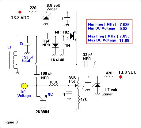
Consider Figure 3. For brevity sake, the VFO buffer stages will not be shown any more but were used in all of the Figures to follow. A single 2N3904 is used as the variable tuning capacitor in this experiment. Note that there are two voltage regulators used on this schematic. If you were really going frugal, only one could also be used. The voltage regulator on the nJFET of the Hartley oscillator is used to lower its operating voltage to minimize the effects of internal heating on this device which can cause drift. Also keeping the RF amplitude down in a PN-junction turned circuit is probably a good idea as large AC voltage swings may cause the PN junction of our tuning device to conduct and reduce Q and waveform purity. You can always build up the oscillator output voltage with buffer/amplifiers.
The second zener diode voltage regulator is used on the voltage control circuit of the tuning circuit. Unregulated voltage for the tuning device whether it is a transistor or diode is not recommended as fluctuations in DC supply voltage will change the frequency of the VFO. Additionally, your DC tuning voltage must be free of any ripple, hum or noise riding along the DC voltage. AC noise if present, can sweep the oscillator frequency at a rate consistent with the ripple frequency. Clean DC power may be achieved by decoupling your VFO power supply from RF with RF chokes, resistors and capacitors. It is also good practice to ensure that correct polarity to your VFO circuit is present at all times.
You can not eliminate the series 100 pF NP0 ceramic capacitor connecting the 2N3904 to the tank circuit or the VFO will not oscillate. You can however, experiment with this capacitor value.
Figure 3 contains the minimum tuning voltage and frequency measured in the test VFO. The capacitance of the 2N3904 will be at its maximum level at the minimum control voltage. The frequency and voltage with the pot turned all the way to the left is 7.036 MHz and 5.82 volts respectively. The minimum control voltage is set by the 47K resistor connecting the 50K pot to ground. Raising this value will raise the minimum control voltage and lowering or eliminating this resistor will lower the control voltage. When the 47K resistor was removed, the measured voltage was 3.42 volts which gave a minimum frequency of 6.977 MHz. From Figure 2 we learned that the minimum voltage should be 7 volts for maximum linearity in the VFO tuning response. I decided to accept 5.82 volts as a trade off to illustrate that in many cases you may compromise the minimum tuning voltage to suit the standard value resistors you have on hand or to attain a bigger tuning range for your VFO. In many design scenarios, compromises may be made to suit your needs and parts collections! The maximum control voltage is largely set by the 11.7 volt zener diode. If you wished to lower this value series resistors or a voltage divider could be added as well. The 11.7 volt zener was chosen as I may want to use this VFO with a 12 volt battery and this zener diode would facilitate such operation. The maximum control voltage and frequency with the pot turned all the way to the right is 7.053 MHz and 11.88 volts. The 2N3904's capacitance would be at its minimum value for this circuit at 11.88 volts. The Figure 3 VFO tuning range is 17 KHz, with the control voltage going from 5.82 to 11.88 volts.
The stability of this VFO is fair. I have a commercial kit receiver that has worse drift, but again I would hesitate to use this VFO design for a transmitter.
One of the drawbacks of using just a single tuning diode or BJT is that if the device is forward biased by the RF signal during part of the AC cycle, it's reverse leakage will increase momentarily and it's Q will be reduced. Also, harmonic energy is produced as the tuning diode or BJT is alternately biased positive and negative which results in reduced VFO output waveform linearity. The solution is to connect two tuning diodes or BJTs back to back with the reverse DC voltage applied to both devices simultaneously. The two tuning diodes will be driven alternately into high and low capacitance and the net capacitance will remain constant and not be affected by the AC signal amplitude. The circuit in Figure 3 could be improved by adding another 2N3904 back-to-back with the existing one, but the tuning range will be reduced. This occurs because you have now connected two capacitors in series and the total capacitance has been reduced and may be analyzed by the classic capacitors in series equation we all learned in radio school. (View)
View full Circuit Diagram | Comments | Reading(1592)
The Test Oscillator
Published:2012/12/6 19:51:00 Author:muriel | Keyword: Test Oscillator
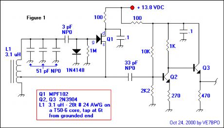
All of the various PN-junction tuning configurations were evaluated in the test oscillator shown in Figure 1. The basic principles and rules of stable low-drift VFO design are still required for the best possible frequency stability. I have covered many of these at the bottom of the following web page from the 40 meter super het project VFO schematic. All the VFO stability hints except for number 6 apply.
When building a PN junction tuned VFO, it is probably best to build the entire VFO, ensure that it is working and then add your tuning circuit. This way you can ensure the circuit oscillates and is stable before you add more circuitry which may make troubleshooting more difficult in the event of problems. I built my test VFO with just the first and second 51 pf NP0 capacitor soldered in place and watched the output in the scope and on the frequency counter. I saw a sine wave and observed the frequency to be ~8.6 MHz. I then soldered the third 51 pf NP0 ceramic capacitor in place and watched the frequency drop to ~7.1 MHz. This is perfect as I wanted my VFO for the 40 meter band and knew that the added tuning circuitry should drop the frequency to somewhere around 7.0 MHz. I listened to the VFO output as an audio tone on my commercial super het tuned to 7.1 MHz after connecting a 1 meter piece of wire to the emitter of Q3 for an antenna . The audio tone after about 5 minutes was quite stable considering the oscillator was not encased in an air tight enclosure. This was also confirmed with the frequency counter. Is is unlikely that the exact same frequency would be measured in a reproduction of this circuit, however it should be close.
The tapped Hartley was chosen for reproducibility and because it is a rare-to-fail design. The voltage across the tank circuit in a Hartley oscillator is many volts peak to peak and I wonder if there is a better VFO design for using tuning diodes with. This web page created much more questions than answers I am afraid.
L1 was wound and then boiled in water for ~6 minutes. It was glued to a single-sided circuit board with Polystyrene Q-Dope from GC Electronics. The coil does not lay on copper as I used a motor tool to grind away the copper in the shape of a circle with a diameter slightly larger than the wound coil. The inductor was doped face down on this circuit and covered with 2 separate coats. It is vital that your inductor is secured so that it is unmovable. A small trimmer variable capacitor for setting the lower band edge frequency would normally be added to this circuit. This was emitted for control purposes when testing the various semiconductors for frequency range in the Figure 1 circuit. The Q2-Q3 buffer has too high an output voltage for 7 dBm diode ring mixers. For diode rings, a more suitable buffer may be used and two examples may be found on this web site. (View)
View full Circuit Diagram | Comments | Reading(2625)
wee willy VFO
Published:2012/12/6 19:50:00 Author:muriel | Keyword: wee willy VFO
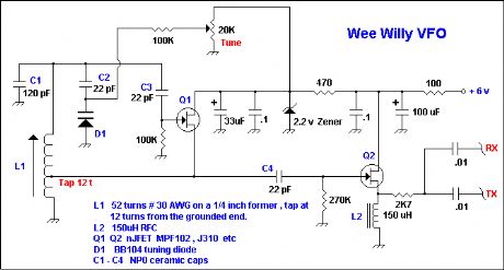
Dick's diagram indicate that this VFO was based upon a design presented in SPRAT for summer 1995. The main inductor L1 is wound with #32 AWG wire on a 1/4 inch slug-tuned coil former. This coil would have an XL somewhere between 250 - 310 ohms, so if you cannot find a coil former as described , you could easily wind one on a powdered iron toroid and make a portion of the C1 capacity variable for adjustment. A suggested alternate inductor is 53 turns of #26 AWG on a T68-6 core powdered iron core.
Dick suggests checking an old television to find suitable coil formers such as the one he used. It would probably be best to distribute the 120 pF C1 capacity among 3-4 capacitors to enhance stability. These caps should be NP0 ceramic for best results with frequency stability.
Dick's oscillator uses the slug tuned core to put VFO frequency close in frequency to where you want to operate and the variable resistor tuner on the front panel allows adjustment around the incoming signal to get the correct pitch. The desired band-edge is easily set by adjusting the slug while listening to the VFO frequency as audio on another receiver that has a frequency readout or directly with a frequency counter.
The L2 150 uH RF choke can be a simple epoxy unit which resembles a resistor. The D1 variable capacitance diode is a BB104 which has ~ 35 pF capacitance on each side. These are available at Dan's Small Parts and Kits whose URL is in the Links section of the site info web page. Experimentation with other tuning diodes could produce a practical alternative to the specified D1 part. (View)
View full Circuit Diagram | Comments | Reading(2033)
wee willy Receiver
Published:2012/12/6 19:48:00 Author:muriel | Keyword: wee willy Receiver
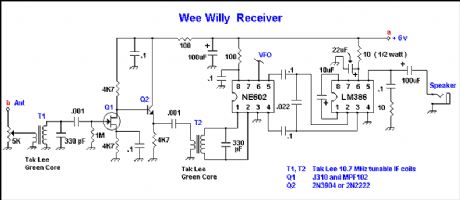
The receiver is a direct conversion type with a manual RF gain control in the form of a 5K potentiometer. Listening to a weak signal on the desired frequency the RF stage and the mixer core ( T1 and T2 ) adjustments are made until you hear the loudest possible signal, keeping the input test signal as low as possible. When the receiver is connected to a doublet antenna there is no lack of incoming signal, which can be controlled by the front panel RF gain control.
The antenna and 6 volt supply is switched manually from TX to RX mode and back by a front panel mounted switch. If you can not find Tak Lee green 10.7 MHz IF coils, probably any other brand of 10.7 MHz slug tuned IF transformer would work. The Mouser catalog number 421F123 would work well and in another 80 meter project I used it with a 470 pF capacitor instead of the 330 pF cap shown. I would start with Dick's 330 pf cap and if it will not tune to resonance sharply, slightly increase the cap value up to see if a bit more capacity is required to resonate it on the desired 75 Meter frequency. Note that the secondary coil on the L1 transformer in the transmitter schematic is unused. If your 10.7 MHz IF coil has a built in capacitor at the base, remove it.
During receive, the standby drain current at 6.0 volts was 24 mA and on loud signals it rose to 100 mA. If this is too much, probably the easiest thing to do would be to put in a series resistor from positive to the LM386 to limit the drain current. To get output on the speaker it is a matter of how loud you want it for the drain you draw. If earphone only reception is okay, then the drain could be reduced considerably. (View)
View full Circuit Diagram | Comments | Reading(4814)
wee willy transmitter
Published:2012/12/6 19:47:00 Author:muriel | Keyword: wee willy transmitter
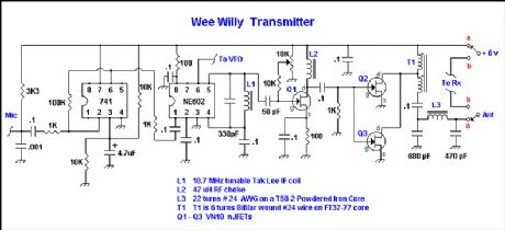
This transmitter uses an electret condenser microphone ( Dick used an Archer 270-90 ). The mic is built right into the front panel of the chassis and this of course guarantees short mic leads. A 741 op amp is used as a speech amplifier which in turn drives the balanced modulator a Signetics NE602 doubly balanced mixer. The input and output impedance of the NE602 mixer is around 1500 ohms.
To adjust the transmitter, set the bias control on the VN10 stage to ground and tweak L1 to resonance using an RF probe or scope on the VN10 input. The input signal must be audio, spoken into the front panel microphone to get the DSB. Once L1 is tuned, connect a 50 ohm load to the antenna with some sort of RF indicator (such as a RF power meter) and advance the bias control to give a watt or so output. Then speaking into the microphone should result in a DSB signal suitable for communicating on QRP! No audio input should result in no RF output. The supplied voltage should be kept at 6 volts, remembering that NE602's cannot stand voltage greater than 9 volts. With suitable voltage control such as a 6.8 volt zener diode on these chips, one could use higher input voltage with a corresponding RF output. (View)
View full Circuit Diagram | Comments | Reading(1837)
Simple Electronic Keyer
Published:2012/12/6 19:45:00 Author:muriel | Keyword: Simple Electronic Keyer
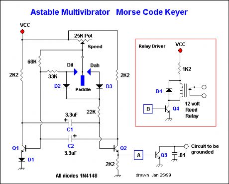
A simple keyer suitable for a popcorn QRP transmitter can be built around an astable multivibrator and an example of such is shown above. The basic design of this keyer is from notes, however the original author of the circuit is unknown. The notes were written in 1973 . I modernized the circuit, added a variable speed control and designed an additional output driver stage.
Keying this circuit generates either dits and spaces or dahs and spaces. When the keyer is idle, Q1 is on and Q2 and Q3 are switched off. When the user sends code, Q1 turns off and Q2 and Q3 switch on and in turn key any device appropriately connected to the collector of Q3. The off-time of Q1 sets the on-time of Q2 and Q3. The off-time of Q2 and Q3 is set by the 22K Q2 base resistor. This off-time is the set time of the spaces and is constant.
The 68K resistor on the base of Q1 is about three times the resistance of the 22K base resistor on Q2 and consequently dahs are ~ three times the length in duration than dits. Spaces and dits are of the same length of time because when sending dits, the 68K base resistor is paralleled with the 33K resistor and effectively the resistance is ~22K ohms. If the optional relay driver transistor Q4 is used instead of Q3, the theory is the same, just substitute Q4 wherever you see Q3. (View)
View full Circuit Diagram | Comments | Reading(2892)
Code Practice Oscillator Project Notes
Published:2012/12/6 19:44:00 Author:muriel | Keyword: Code Practice Oscillator
The voltage / time output waveform of the astable multivibrator is largely a square wave which some people find harsh. Many users prefer listening to a sine wave although that is beyond the scope of this web page. The multivibrator shown has real advantages in that, it is both dependable and tolerant with respect to parts substitutions. Keying the oscillator as shown practically guarantees that the multivibrator will start running each time you hit the key.
VCC can be 9 to 13.8 volts DC and the larger the voltage the greater the volume in the headphones. The B+ decoupling circuit at the top left can be omitted for battery operation or if you prefer not to bother with it. The basic multivibrator and emitter-follower circuit can be used in a transceiver as a sidetone for monitoring keying. A series resistor from the emitter-follower maybe necessary to attenuate/match the sidetone to the transceiver's AF amp.
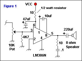
If you desire speaker level output, the Q5 common-collector final can be omitted and the circuit shown below used. This circuit uses the LM386N and provides up to ~ 0.5 watts into an 8 ohm speaker. Connect the Figure 1 circuit as shown to the 10 uF coupling capacitor connected to the collector of Q4. Do not connect the 10 ohm half-watt resistor to the decoupled VCC shown in the schematic. The power supply to the LM386N AF amp should be directly connected to the VCC, not like the common-collector AF stage shown in the schematic to the right. (View)
View full Circuit Diagram | Comments | Reading(1033)
Code Practice Oscillator
Published:2012/12/6 19:43:00 Author:muriel | Keyword: Code Practice Oscillator
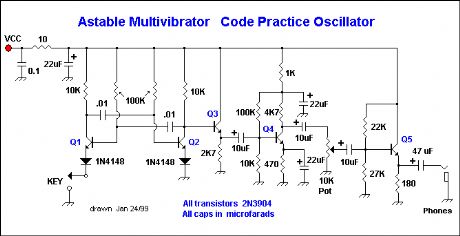
View full Circuit Diagram | Comments | Reading(3490)
VFO Design
Published:2012/12/6 19:40:00 Author:muriel | Keyword: VFO Design
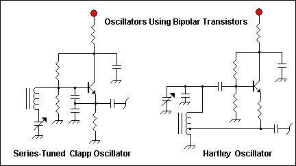
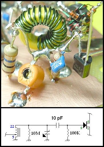
Reviewing the Amateur Radio literature revealed that JFETS enjoy tremendous popularity as the active device in LC local oscillators during the past ten years. To conform to the original design criteria of this project it was decided to build the VFO from only 2N3904s for the oscillator and the buffer sections. Four different VFO's were built and tested for short and long term frequency stability. Two partial schematics are shown below. Each design used the same buffer/amplifier for some sort of control. I found that it is possible to build very stable oscillators using the 2N3904, providing good quality, temperature-stable components are used. Careful attention to the design guidelines published by people like W1FB, W7EL and W7ZOI are mandatory. Electrical engineering knowledge would also be very helpful as I found biasing and feedback resistance values, coupling cap values and inductor Q all can have an effect on frequency stability and/or output noise.
My tests failed to determine why the JFET is so popular; there are just too many variables to factor in both electronically and through building techniques. Possibly, the easiest no-fail VFO to build is the tapped inductor Hartley using a JFET and this may help explain the popularity of the JFET.
This design was by far the most stable design for both short and long term drift and is the most stable VFO that I have ever built. The VFO will see duty as a lab oscillator for use in future projects built for the great QRP band, 30 meters.
Despite the fact that the oscillators built with the bipolar transistors were frequency stable, 1 VFO stood out -- the VFO circuit entitled: An (LC) VFO for 30 Meters (View)
View full Circuit Diagram | Comments | Reading(1686)
Product Detector
Published:2012/12/6 19:39:00 Author:muriel | Keyword: Product Detector
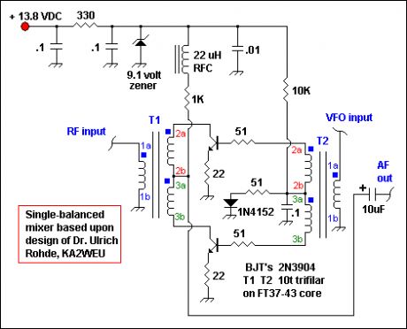
A product detector using either one or more 2N3904 transistors was originally planned and indeed, four designs were built and tested. The 2 favorite detectors were a single-ended detector built with a single BJT which maybe used in an future novelty transceiver project and a passive mixer invented by Dr. Ulrich Rohde. The original mixer called for 2N5179 transistors and used a 0.1 uF coupling cap to the diplexer stage for RF output. It should have a VCC of 9 volts DC.
The mixer as built for this project is shown to the right.
The mixer as designed by Rohde had a reported IP3 of 33 dBm with a LO drive of 15-17 dBm and an insertion loss of ~ 6dB. This mixer operates in push-pull and the 22 ohm resistors on the transistor emitters provide degenerative feedback which makes component matching unnecessary. The schematic and brief write up can be found in QST for June 1994 in an article entitled Key Components of Modern Receiver Design-Part 2. See references 1 and 2.
I built 2 versions of Rohde's mixer and tested them both in the receiver shown in the main schematic. I later discarded this design and replaced it with the familiar diode ring mixer for the following subjective reasons; I noted a greater insertion loss, more hum and noise, higher LO drive level requirements and more WWV AM interference when compared to a diode ring mixer.
No quantitative measurements of the mixer were made. Listening tests and observations were only performed. Careful shielding of one version of the mixer resulted in a major improvement in hum and obliteration of an audio feedback problem noted when the AF gain was increased maximally when compared to the unshielded second version of the mixer. In addition, better performance would most certainly be realized if 2N5179 BJT's had been used instead of 2N3904's. Rohde's mixer certainly warrants further and better analysis with quantitative testing for use in home built receivers.
If you build and test this mixer, please forward or publish the results for use by the Amateur Radio community. The trifilar wound transformers are identical to those shown elsewhere on this site and have phasing dots and coil numbering included for reference. Ugly constructing this mixer is extremely easy to do. The diode ring mixer ultimately used has 50 ohm ports and can be a homebrew or commercial unit such as the popular SBL-1 from Mini-Circuits. (View)
View full Circuit Diagram | Comments | Reading(0)
Band pass Filter
Published:2012/12/6 19:39:00 Author:muriel | Keyword: Band pass Filter
A band pass filter was designed for low insertion loss to help maintain the receiver noise figure. In keeping with this, NP0 ceramic capacitors were used for the 68 pF and 5 pF fixed-value capacitors. The trimmer cap was a 5 -20 pF ceramic variable with a Qu of 300. (Digi-Key bottom-adjusted SG20016-ND). The leads were bent so that each trimmer cap could be adjusted from the top. The L1 and L2 inductors were wound using 27 turns of #26 AWG enamel coated wire on T50-6 powdered iron toroids. A tap was made four turns up from the grounded end. Qu is ~ 250 for these inductors. The center frequency is 10.125 MHz, the bandwidth is 0.88 MHz and the loaded Q of the resonators is 11.5. The easiest method to tune the resonators is to peak the trimmer caps for the greatest measured output voltage using an oscilloscope. I used the receiver VFO temporarily terminated with a -10dB, 50 ohm pad to obtain the correct filter input impedance and connected it to the input end of the filter. I temporarily terminated the output of the filter with a 51 ohm resistor to ground. The VFO was tuned to the center frequency by placing it next to a receiver set on 10.125 MHz. A frequency counter can also be used. The trimmers were adjusted on each resonator to obtain the highest measured voltage possible. The filter was then placed in the receiver after removing the temporary alterations used during calibration. If you do not have access to test equipment, tune the resonators at the center frequency while listening to the receiver in the headphones to obtain the greatest possible band noise. Confirm your adjustments by tweaking the trim caps while listening to a QSO as well.
(View)
View full Circuit Diagram | Comments | Reading(1953)
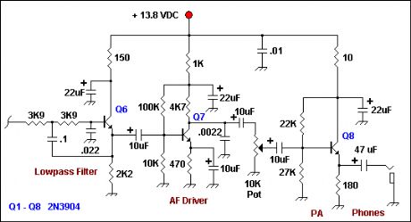
30 Meter Receiver
Published:2012/12/6 1:38:00 Author:muriel | Keyword: 30 Meter, Receiver
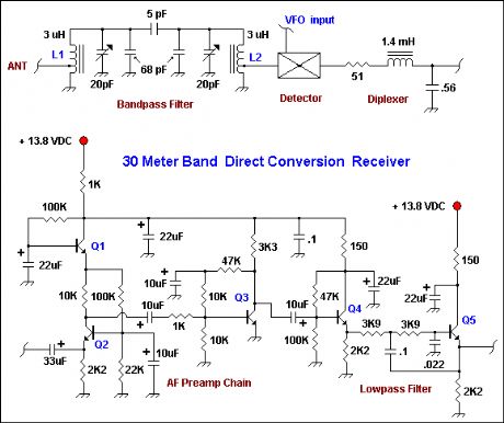
A lot can be learned when using strict design criteria to build a project. I set out to build an entire receiver using only 2N3904 transistors and at the end settled upon the design shown above. This design resembles that of the Ugly Direct receiver on this web site in a lot of ways and is also a low-cost popcorn project. A great deal of time was spent building and testing various VFO designs and investigating an interesting single-balanced mixer using two 2N3904 BJT's. The design process and reasons for abandoning my original criteria in the case of the mixer and VFO will be discussed. (View)
View full Circuit Diagram | Comments | Reading(1078)
Ugly Construction
Published:2012/12/6 1:36:00 Author:muriel | Keyword: Ugly Construction
View full Circuit Diagram | Comments | Reading(1065)
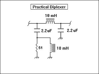
Practical Diplexer for Popcorn Receivers
Published:2012/12/6 1:35:00 Author:muriel | Keyword: Practical Diplexer , Popcorn Receivers
View full Circuit Diagram | Comments | Reading(1420)
Comments and analysis by W7ZOI
Published:2012/12/6 1:34:00 Author:muriel | Keyword: Comments , analysis, W7ZOI
View full Circuit Diagram | Comments | Reading(888)
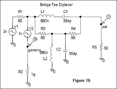
Bridge-Tee RF Diplexer
Published:2012/12/6 1:33:00 Author:muriel | Keyword: Bridge-Tee RF Diplexer
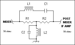
This is an excellent bandstop/bandpass diplexer popularized by Joe Reisert W1JR. This easy to build diplexer has a low parts count and is easily built using Ugly Construction. Resistors R1 and R2 present a 50 ohm impedance to the mixer output and a 50 ohm impedance to the input of the post mixer amplifier. The IF frequency is passed through the diplexer while out of passband RF is given a low impedance path to ground. The capacitance for C1 is generally built up by substituting the nearest standard value capacitor or by placing 2 or more capacitors in parallel with each other to achieve the desired value. The same procedure is then repeated for the C2 capacitance. For more strenuous purposes, a portion of C1 and C2 or the inductors L1 and L2 can be variable and adjusted on the bench. The inductors can easily wound on powdered-iron toroid cores. I have used T50-2 or T50-6 type toroids with good results. The Q of the inductors is 1.It is possible to design a more generalized form of this diplexer with a higher loaded Q in the resonators. The diplexer shown and used in the program has a Q of 1. This was used by W1JR in his VHF/UHF World Column in the now defunct HAM Radio Magazine for March and November 1984. It was also more recently used by Jacob Makhinson, N6NWP in his A High-Dynamic Range MF/HF Receiver Front End in QST for February 1993. The actual formulae for this diplexer is far more complex than the simplified formula shown below or used in the program, but both provide a very good approximation for the Q = 1 version as used by W1JR and N6NWP. If you wanted Q=10, the series tuned circuit would use L that is 10 times as high with C to resonate. The parallel tuned circuit would then use C that was 10 times higher with L to resonate. A supplemental web page with some hard-core mathematics for this diplexer can be found on the Diplexer Supplemental Page. (View)
View full Circuit Diagram | Comments | Reading(2920)
| Pages:251/2234 At 20241242243244245246247248249250251252253254255256257258259260Under 20 |
Circuit Categories
power supply circuit
Amplifier Circuit
Basic Circuit
LED and Light Circuit
Sensor Circuit
Signal Processing
Electrical Equipment Circuit
Control Circuit
Remote Control Circuit
A/D-D/A Converter Circuit
Audio Circuit
Measuring and Test Circuit
Communication Circuit
Computer-Related Circuit
555 Circuit
Automotive Circuit
Repairing Circuit