
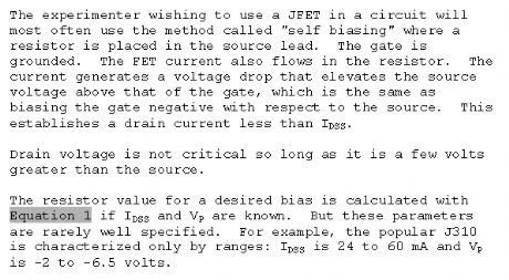
Circuit Diagram
Index 250
Multi-channel pressure XMD diagram
Published:2012/12/7 1:19:00 Author:Ecco | Keyword: Multi-channel, pressure XMD
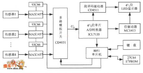
It uses multi-chip MAX1457 to match with single-chip A / D converter and SCM, then they constitute a multi-channel pressure XMD, and the circuit diagram is shown in Fig. In the figure, it uses 8-to-1 analog switch CD4051 to receive up to 8-channel sensor signals. Each sensor calibration coefficients are stored in the 93C66. CD4051 output connects to ICL7135 - 4 1/ 2 single-chip A / D converter, then it can 41 / 2 digit LED display by decoder driver(CD4511) and bit driver (MC1413).
(View)
View full Circuit Diagram | Comments | Reading(1219)
Tms320f2812 dsp controller - based electric circuit diagram
Published:2012/12/7 0:58:00 Author:Ecco | Keyword: dsp controller, electric
Tms320f2812 dsp controller - based electric circuit diagram is shown in figure.
(View)
View full Circuit Diagram | Comments | Reading(958)
Two kinds of output switching power supply circuit diagram
Published:2012/12/7 1:24:00 Author:Ecco | Keyword: output , switching power supply
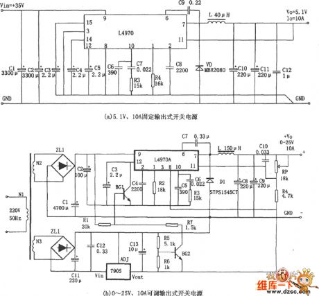
As shown in figure, it is a high-power switching power supply with L4970A. L4970A is a high-power single-chip switch integrated voltage regulator, the chip uses SIP-15 package, which is characterized by: ( 1 ) Input voltage must be > 11V, and the value is typically between 15 ~ 40V; ( 2 ) Output voltage: Fixed output is 5.1V, and it can also be set through an external circuit adjustable output with the range of 5.1 ~~ 40V; ( 3 ) the maximum output current is 10A; ( 4 ) operating frequency is 200kHz; ( 5 ) internal undervoltage detection, brownout reset power stage soft start circuit.
(View)
View full Circuit Diagram | Comments | Reading(1775)
Step-up switching regulator power supply circuit
Published:2012/12/7 1:41:00 Author:Ecco | Keyword: Step-up , switching regulator , power supply
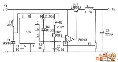
In the circuit, It uses transistor BG1 as a switching adjust tube; operational amplifier IC1 constitutes the compare amplifier; 555 time-base circuit is connected as astable multivibrator. Oscillator produces a sawtooth voltage on C1 (Vmin = 1/3Vz, Vmax = 2/3Vz, the frequency is determined by W1 and C1 ), then it is supplied to the noninverting input of the comparator IC1, sampling voltage is supplied to the inverting input terminal of comparator. The duty cycle of the rectangular waveform output by IC1 is decided by the sampling voltage, when the output voltage is a stable value, the sampled voltage is between 1/3Vz and 2/3Vz.
(View)
View full Circuit Diagram | Comments | Reading(3491)
Optocoupler output mode circuit diagram of switching power supply
Published:2012/12/7 0:56:00 Author:Ecco | Keyword: Optocoupler , output mode , switching power supply
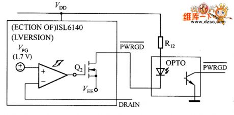
The PWRGD output port of power supply can display the input state of external power supply, and it is shown in Figure 1.
(View)
View full Circuit Diagram | Comments | Reading(1244)
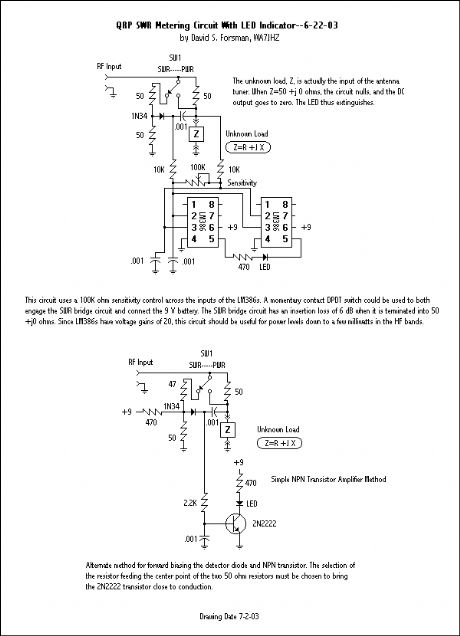
QRP SWR Meter With LED Indicator
Published:2012/12/6 20:21:00 Author:muriel | Keyword: QRP SWR Meter, LED Indicator
View full Circuit Diagram | Comments | Reading(3648)
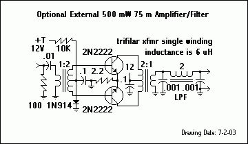
optional external 500mW 75m amplifier/filter
Published:2012/12/6 20:20:00 Author:muriel | Keyword: optional external , 500mW , 75m , amplifier, filter
View full Circuit Diagram | Comments | Reading(983)
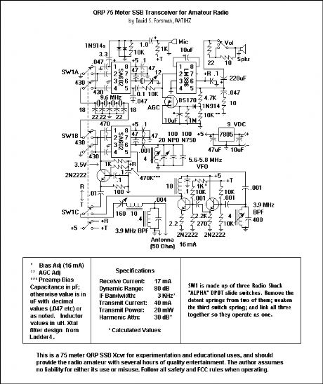
QRP 74 meter SSB Transceiver
Published:2012/12/6 20:19:00 Author:muriel | Keyword: QRP 74 meter, SSB Transceiver
View full Circuit Diagram | Comments | Reading(1404)
SSB 75 Meter Transceiver
Published:2012/12/6 20:18:00 Author:muriel | Keyword: SSB 75 Meter, Transceiver
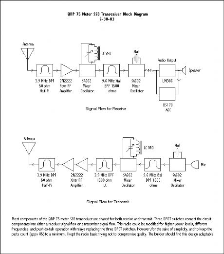
View full Circuit Diagram | Comments | Reading(748)
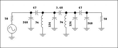
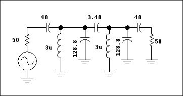
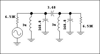
LC Bandpass Filters 3
Published:2012/12/6 20:17:00 Author:muriel | Keyword: LC Bandpass Filters
View full Circuit Diagram | Comments | Reading(807)
LC Bandpass Filters 2
Published:2012/12/6 20:16:00 Author:muriel | Keyword: LC Bandpass Filters
View full Circuit Diagram | Comments | Reading(1052)
LC Bandpass Filters
Published:2012/12/6 20:16:00 Author:muriel | Keyword: LC Bandpass Filters
View full Circuit Diagram | Comments | Reading(749)
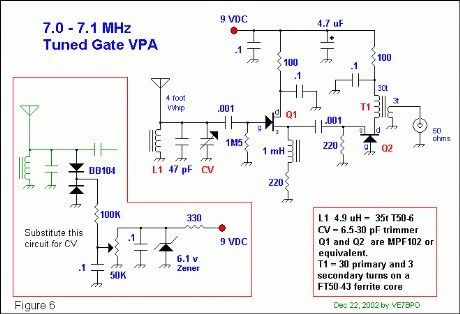
7.0-7.1MHz tuned gate VPA
Published:2012/12/6 20:14:00 Author:muriel | Keyword: 7.0-7.1MHz , tuned gate VPA
View full Circuit Diagram | Comments | Reading(904)
VPA High Pass/Low Pass Filter after Q1 Stage
Published:2012/12/6 20:13:00 Author:muriel | Keyword: VPA , High Pass/Low Pass, Filter, Q1 Stage
View full Circuit Diagram | Comments | Reading(1024)
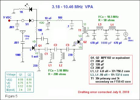
VPA With A High Pass Filter After The Q1 Stage
Published:2012/12/6 20:13:00 Author:muriel | Keyword: VPA , High Pass Filter, Q1 Stage
View full Circuit Diagram | Comments | Reading(1088)
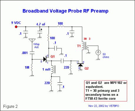
broadband voltage probe RF preamp
Published:2012/12/6 20:12:00 Author:muriel | Keyword: broadband voltage , probe RF preamp
View full Circuit Diagram | Comments | Reading(2236)
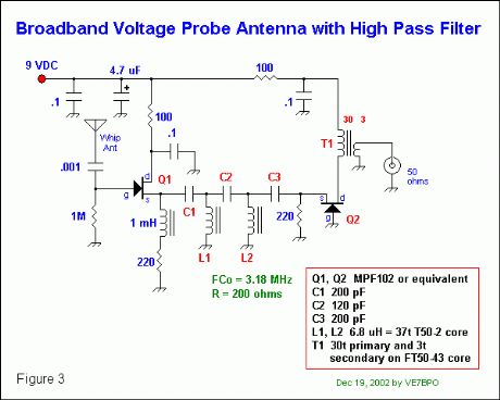
Broadband Voltage Probe Antennas
Published:2012/12/6 20:11:00 Author:muriel | Keyword: Broadband Voltage, Probe Antennas
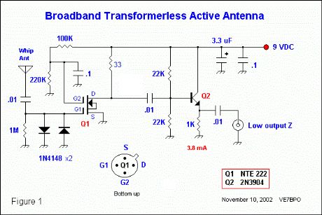
Figure 1 and Picture 1 shows the respective schematic and outcome for the first broadband version I constructed. This is similar to a version sold as a kit, except for the Q2 stage, which was added to decrease the output impedance to preserve the function of my receiver double tuned filter stage. (View)
View full Circuit Diagram | Comments | Reading(2216)
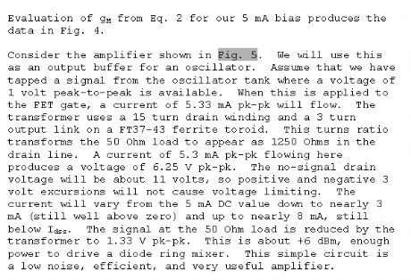
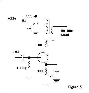
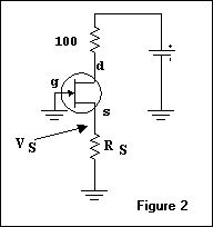
Common source amplifier biased for 5 mA drain current
Published:2012/12/6 20:08:00 Author:muriel | Keyword: Common source amplifier, 5 mA , drain current.
View full Circuit Diagram | Comments | Reading(801)
Data used to produce transconductance for the FET used in our sample amplifier.
Published:2012/12/6 20:07:00 Author:muriel | Keyword: Data, produce transconductance, FET, sample amplifier.
View full Circuit Diagram | Comments | Reading(732)
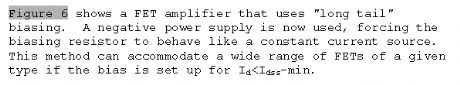
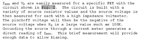
Basic behavior of an N-Channel depletion mode JFET
Published:2012/12/6 20:06:00 Author:muriel | Keyword: N-Channel , depletion mode, JFET
View full Circuit Diagram | Comments | Reading(900)
| Pages:250/2234 At 20241242243244245246247248249250251252253254255256257258259260Under 20 |
Circuit Categories
power supply circuit
Amplifier Circuit
Basic Circuit
LED and Light Circuit
Sensor Circuit
Signal Processing
Electrical Equipment Circuit
Control Circuit
Remote Control Circuit
A/D-D/A Converter Circuit
Audio Circuit
Measuring and Test Circuit
Communication Circuit
Computer-Related Circuit
555 Circuit
Automotive Circuit
Repairing Circuit