
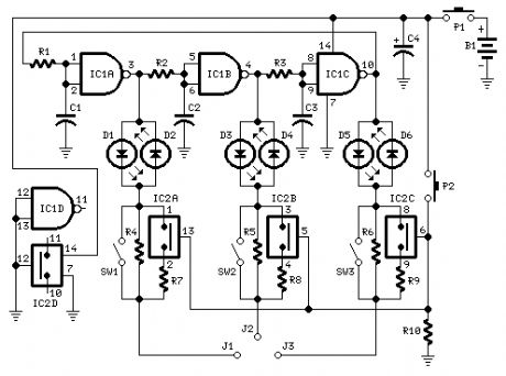
Measuring and Test Circuit
Index 14
E-B-C Transistor Pin Identifier
Published:2012/12/23 20:58:00 Author:muriel | Keyword: E-B-C Transistor, Pin Identifier
View full Circuit Diagram | Comments | Reading(1748)
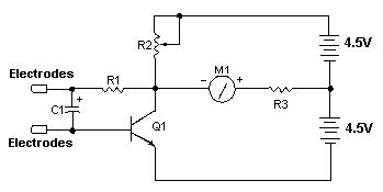
Sound Pressure Level Meter
Published:2012/12/20 20:55:00 Author:muriel | Keyword: Sound Pressure Level, Meter
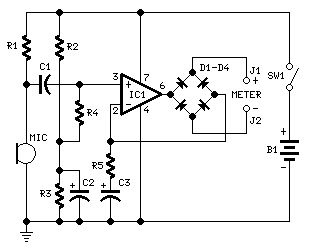
View full Circuit Diagram | Comments | Reading(1601)
product detector 3
Published:2012/12/16 21:11:00 Author:muriel | Keyword: product detector
View full Circuit Diagram | Comments | Reading(1385)
product detector 2
Published:2012/12/16 21:11:00 Author:muriel | Keyword: product detector
View full Circuit Diagram | Comments | Reading(1476)
Band pass Filter and Product Detector
Published:2012/12/16 21:08:00 Author:muriel | Keyword: Band pass Filter, Product Detector
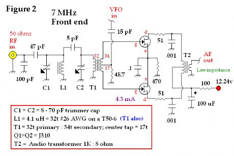
View full Circuit Diagram | Comments | Reading(1881)
Third RF Amplifier Stage and Detector
Published:2012/12/14 20:46:00 Author:muriel | Keyword: Third , RF Amplifier Stage, Detector
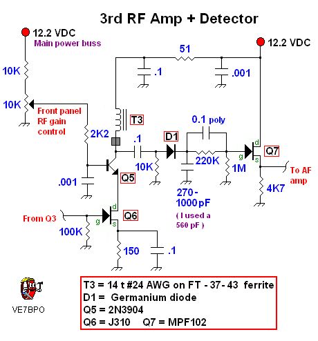
View full Circuit Diagram | Comments | Reading(1510)
L-Match AM Detector
Published:2012/12/13 21:30:00 Author:muriel | Keyword: L-Match, AM Detector
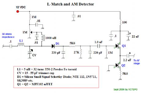
View full Circuit Diagram | Comments | Reading(1800)
VK4FUQ AM detector
Published:2012/12/13 21:28:00 Author:muriel | Keyword: VK4FUQ , AM detector
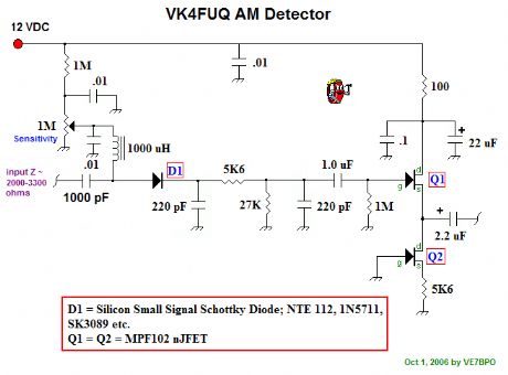
View full Circuit Diagram | Comments | Reading(1798)
Cut Phone Line Detector
Published:2012/12/12 0:41:00 Author:muriel | Keyword: Cut Phone Line, Detector

View full Circuit Diagram | Comments | Reading(873)
Sound Level Meter 2
Published:2012/12/12 0:30:00 Author:muriel | Keyword: Sound Level Meter
View full Circuit Diagram | Comments | Reading(1200)
The analog phase detector circuit diagram with 0.1 % gain accuracy
Published:2012/12/11 1:04:00 Author:Ecco | Keyword: analog phase , detector , 0.1 % gain accuracy
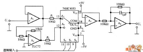
It is composed of operational amplifier TLC072 and analog switch 74HC4053, but analog switch conduction resistance changes with temperature and power supply voltage. In the circuit, analog switch 74HC4O53 output is connected to a voltage follower composed of A3, therefore, conduction resistance does not affect the output. If the input signal source impedance is very low, you can not connect A1. 74HC series can not guarantee the picking up firstly, even if 74HC4053 makes A2 and A2 short-circuit, the additional resistors R1 and R2 prevent problem in the practical use.
(View)
View full Circuit Diagram | Comments | Reading(5481)
Water Detector With Sump/Bilge Pump Controller
Published:2012/12/11 0:34:00 Author:muriel | Keyword: Water Detector, Sump/Bilge, Pump Controller
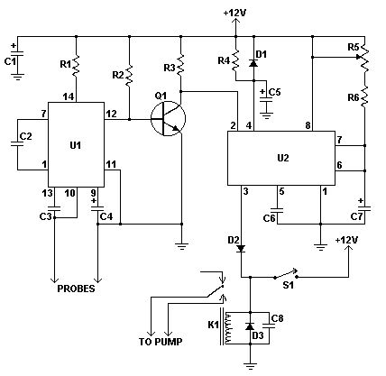
This moisture detector with pump controller is built around the special purpose LM1830 IC. The LM1830 is designed to detect moisture by passing an AC current through a set of probes. An internal comparator compares the resistance of the probes to an internal reference. When the resistance between the probes is low (indicating the presence of water or other conductive liquid) then the IC triggers it's output. An AC signal avoids electroplating and corrosion problems that are common when DC is used. To provide an adjustable delay hysteresis to avoid cycling the pump, a timer based around the 555 is used a range of about 5 seconds to two minutes. In this way the pump will stay active for a set amount of time even if the fluid level is below that of the probes. (View)
View full Circuit Diagram | Comments | Reading(2169)
Simple Polarity Tester
Published:2012/12/11 0:27:00 Author:muriel | Keyword: Simple Polarity, Tester
View full Circuit Diagram | Comments | Reading(1154)
Simple Lie Detectors
Published:2012/12/11 0:27:00 Author:muriel | Keyword: Simple Lie, Detectors
Here's a simple lie detector that can be built in a few minutes, but can be incredibly useful when you want to know if someone is really telling you the truth. It is not as sophisticated as the ones the professionals use, but it works. It works by measuring skin resistance, which goes down when you lie.
(View)
View full Circuit Diagram | Comments | Reading(959)
Air Flow Detector
Published:2012/12/11 0:23:00 Author:muriel | Keyword: Air Flow, Detector
View full Circuit Diagram | Comments | Reading(0)
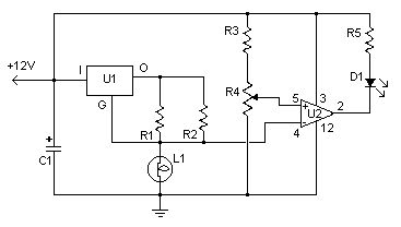
Light/Dark Detector
Published:2012/12/10 1:00:00 Author:muriel | Keyword: Light/Dark Detector
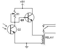
View full Circuit Diagram | Comments | Reading(896)
EMF Field Intensity Meter
Published:2012/12/10 0:41:00 Author:muriel | Keyword: EMF, Field Intensity Meter
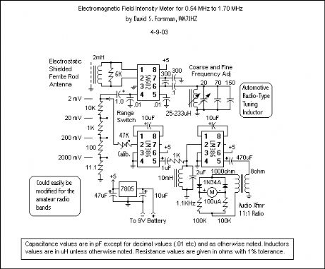
View full Circuit Diagram | Comments | Reading(1863)
Multi-channel pressure XMD diagram
Published:2012/12/7 1:19:00 Author:Ecco | Keyword: Multi-channel, pressure XMD
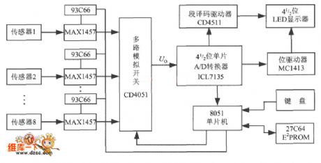
It uses multi-chip MAX1457 to match with single-chip A / D converter and SCM, then they constitute a multi-channel pressure XMD, and the circuit diagram is shown in Fig. In the figure, it uses 8-to-1 analog switch CD4051 to receive up to 8-channel sensor signals. Each sensor calibration coefficients are stored in the 93C66. CD4051 output connects to ICL7135 - 4 1/ 2 single-chip A / D converter, then it can 41 / 2 digit LED display by decoder driver(CD4511) and bit driver (MC1413).
(View)
View full Circuit Diagram | Comments | Reading(1215)
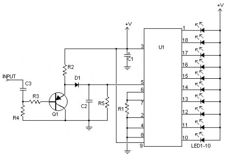
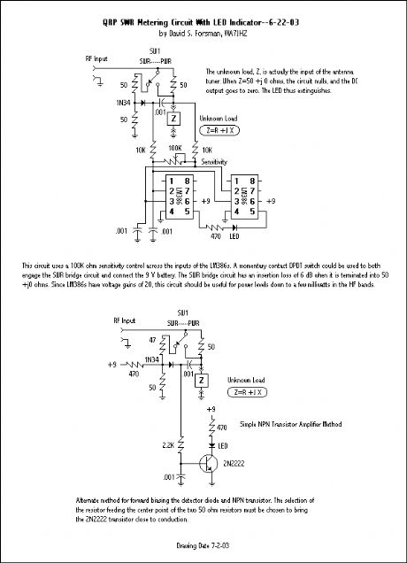
QRP SWR Meter With LED Indicator
Published:2012/12/6 20:21:00 Author:muriel | Keyword: QRP SWR Meter, LED Indicator
View full Circuit Diagram | Comments | Reading(3642)
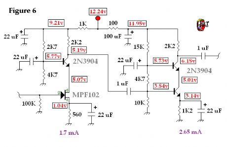
The Test Oscillator
Published:2012/12/6 19:51:00 Author:muriel | Keyword: Test Oscillator
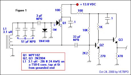
All of the various PN-junction tuning configurations were evaluated in the test oscillator shown in Figure 1. The basic principles and rules of stable low-drift VFO design are still required for the best possible frequency stability. I have covered many of these at the bottom of the following web page from the 40 meter super het project VFO schematic. All the VFO stability hints except for number 6 apply.
When building a PN junction tuned VFO, it is probably best to build the entire VFO, ensure that it is working and then add your tuning circuit. This way you can ensure the circuit oscillates and is stable before you add more circuitry which may make troubleshooting more difficult in the event of problems. I built my test VFO with just the first and second 51 pf NP0 capacitor soldered in place and watched the output in the scope and on the frequency counter. I saw a sine wave and observed the frequency to be ~8.6 MHz. I then soldered the third 51 pf NP0 ceramic capacitor in place and watched the frequency drop to ~7.1 MHz. This is perfect as I wanted my VFO for the 40 meter band and knew that the added tuning circuitry should drop the frequency to somewhere around 7.0 MHz. I listened to the VFO output as an audio tone on my commercial super het tuned to 7.1 MHz after connecting a 1 meter piece of wire to the emitter of Q3 for an antenna . The audio tone after about 5 minutes was quite stable considering the oscillator was not encased in an air tight enclosure. This was also confirmed with the frequency counter. Is is unlikely that the exact same frequency would be measured in a reproduction of this circuit, however it should be close.
The tapped Hartley was chosen for reproducibility and because it is a rare-to-fail design. The voltage across the tank circuit in a Hartley oscillator is many volts peak to peak and I wonder if there is a better VFO design for using tuning diodes with. This web page created much more questions than answers I am afraid.
L1 was wound and then boiled in water for ~6 minutes. It was glued to a single-sided circuit board with Polystyrene Q-Dope from GC Electronics. The coil does not lay on copper as I used a motor tool to grind away the copper in the shape of a circle with a diameter slightly larger than the wound coil. The inductor was doped face down on this circuit and covered with 2 separate coats. It is vital that your inductor is secured so that it is unmovable. A small trimmer variable capacitor for setting the lower band edge frequency would normally be added to this circuit. This was emitted for control purposes when testing the various semiconductors for frequency range in the Figure 1 circuit. The Q2-Q3 buffer has too high an output voltage for 7 dBm diode ring mixers. For diode rings, a more suitable buffer may be used and two examples may be found on this web site. (View)
View full Circuit Diagram | Comments | Reading(2626)
| Pages:14/101 1234567891011121314151617181920Under 20 |
Circuit Categories
power supply circuit
Amplifier Circuit
Basic Circuit
LED and Light Circuit
Sensor Circuit
Signal Processing
Electrical Equipment Circuit
Control Circuit
Remote Control Circuit
A/D-D/A Converter Circuit
Audio Circuit
Measuring and Test Circuit
Communication Circuit
Computer-Related Circuit
555 Circuit
Automotive Circuit
Repairing Circuit