
Signal Processing
Index 36
1W fm transmitter circuit
Published:2012/10/11 2:20:00 Author:muriel | Keyword: 1W, fm transmitter

A very good 1 watt fm transmitter circuit, very easy to build circuit. It has 4 transistors, one is a very stable oscillator, followed by a buffer stage to prevent frequency variation when you adjust the transmitter. Next is a resonance stage and the final stage built with a minimum 1W transistor which must have a heatsink. You must use a LM7805 stabilizer for the oscillator diodes and one LM7809 for powering up the T1 oscillator stage. This will give you a very stable transmitter frequency.
1W FM Transmitter Circuit Diagram
First build the oscillator stage and the buffer, power it up and trim the 10k linear potentiometer untill you can here a blank signal on your receiver. If you put a small piece of wire on the T2 emitter you can see that the cover range of the 2 stage transmitter is about 3 meter.
After you are sure that your oscillator+buffer stage are working properly, remove the power supply and continue building the T3 resonance stage. Connect the power supply and if you adjust the trimmer (variable capacitor) from T3 collector you can see how the fm transmitter power can be varied. This stage is very important for proper functionality of the entire 1 watt fm transmitter. You must adjust the trimmer for maximum power.
1 Watt fm transmitter adjustment
The final stage of the 1W fm transmitter is built with 2N4427 (recommended) or the transistors from the list. If you can’t find any, use a BD139 transistor but only for frequencies lower than 90 MHz. The output power will be lower but you get the idea. If you decide to use 2N2219 transistor for the final stage of the transmitter you must know that the output rf power will be 0.4W.
Adjust the last 2 trimmers for maximum output power in the antenna. Initially use 2 x 100 Ω 0.5W resistors in parallel at the RF output. Then connect this rf probe to the output and adjust all the 3 trimmers starting from T3 to output. You must adjust it to obtain the maximum multimeter indication. Then power it off, connect the antenna and make the final adjustments for maximum broadcasting coverage distance.
The oscillator and buffer stage must be enclosed in a 1 mm copper case, then do the same with the T3 and T4 stages.
Use a 12Vdc power supply to power up this fm broadcast circuit. T4 will have a current consumption of around 150 mA at full power output adjustments. The total current consumption of the entire 1 watt transmitter will be around 500 mA. (View)
View full Circuit Diagram | Comments | Reading(1548)
PLL transmitter circuit
Published:2012/10/10 2:00:00 Author:muriel | Keyword: PLL transmitter
The PLL transmitter exciter has the functions of providing a stable, low noise, frequency-selectable RF signal and amplify it to a controllable output power sufficient to drive the power amplifier. It uses a PLL frequency synthesizer built with MC145151, which covers the FM band in 100kHz steps. The VCO covers only a few MHz without readjustment. The pll transmitter output power is controllable from zero to 4 watts. A PLL unlock detector is included, to shut down the transmitter in the event of a malfunction. The Colpitts VCO is powered from a local 9V regulator, and has the frequency controlled by two back-to-back varactors, resulting in minimal loading and thus ultra low phase noise.
The output of the VCO goes through an emitter follower buffer stage, then through a broadly tuned class A amplifier, followed by a class B driver and a class C power amplifier, which use medium-Q tuned impedance matching networks. These last two stages are powered from a separate input, so that the output power of the Phase-Locked Loop transmitter can be controlled from zero to 4 W by adjusting this voltage from zero to 15V.
Note that the output of this pll module does not have enough harmonic filtering to connect it directly to an antenna. If you want to use this exciter as a stand-alone low power transmitter, you should add a low pass filter.
PLL transmitter circuit diagram
Phase-Locked Loop transmitter PCB
The Phase-Locked Loop transmitter is built on a double sided PCB, which has its top side copper left mostly undisturbed as a ground plane. The copper is removed only around non-grounded pins. The ground connections are soldered on the top side, so it’s not necessary to have plated-through holes.
This drawing shows the two sides of the PCB, so that you can print it and fold it in the middle to see how the two parts align. You will have to invert the image to print it for making the board, so that the ink gets in contact with the copper. This PCB is fitted with soldered shields all around and between stages, on both sides of the board. They are best installed before populating it. (View)
View full Circuit Diagram | Comments | Reading(929)
FM Radio Transmitter circuit
Published:2012/10/10 1:59:00 Author:muriel | Keyword: FM, Radio Transmitter
A simple fm radio transmitter circuit which covers frequencies from 88 to 108 MHz. It is built with 3 transistors: BC109, BFR91A and BFR96S. It is quite stable and the output power is around 200 mW.
The first stage in a mic amplifier but if you connect this radio transmitter directly to an audio source you can remove this stage and connect the audio signal to R5.U1, 1PH51C can be replaced with LM7805. You must use a stabilized power source for oscillator stage to prevent frequency variation. You can remove C7 and use a linear potentiometer insted of R6 with the median connector to C4, one pin to ground and the other one to +. You may replace BB109 varicap diode with BB139.
All coils must be perpendicular one to the other, especially L2 and L3. The oscillator stage must be encased with a copper 1mm foil. If you use an external antenna, like this fm dipole antenna connect it with a good coaxial cable because the power is low and you want to use most of it. If you don’t want to loose the rf power connect the radio transmitter close to the antenna (2 meter coaxial cable) and use a longer cable for the audio signal (coaxial). If you connect the antenna as I told you before you can cover a 300 meter in diameter area.
FM Radio Transmitter Circuit Diagram
(View)
View full Circuit Diagram | Comments | Reading(1754)
Signal generator with thyristor
Published:2012/10/10 1:56:00 Author:muriel | Keyword: Signal generator
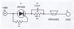
A very simple thyristor signal generator circuit which uses a single thyristor, two resistors, a capacitor and a mini-loudspeaker. Once the circuit is switched ti a current source, current flows through R1 and switches on the thyristor. The thyristor conducts current and chargers capacitor C.Since the charging current is inversely proportional to the charging of the capacitor, it slowly decreases until such a level that the thyristor switches off. Once the thyristor is off, capacitor C discharges through R2 and the whole process is repeated. The periodice switching on and off of the thyristor generates the oscillating signal. The frequency of the oscillation is determined by the C/R2 combination.
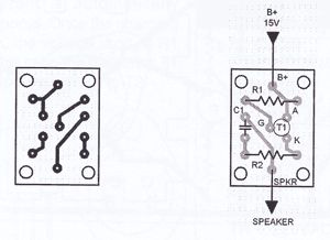
Signal generator circuit diagram and PCB layout
(View)
View full Circuit Diagram | Comments | Reading(1198)
Veronica 1W Fm transmitter circuit
Published:2012/10/10 1:51:00 Author:muriel | Keyword: 1W, Fm transmitter
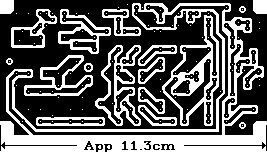
Veronica 1W FM transmitter is easy to build and to operate in FM. Veronica is also known for frequency stability, clean fm signal and uses no integrated circuit.You may want to check this another 1W FM transmitter circuit.Veronica transmitter is equiped with a mini-mixer and so you may forget an external mixer. This consist from T1 transistor wich amplifies the microphone signal before it is combined with cd-player audio or pc signal. R1 and R2 are potentiometers ( variable resistors ) used to adjust the audio level.The component between R8 and C21 represents the oscillator wich generates radio signal. D1 is a varicap diode ( like a variable capacitor or trimmer) controlled by audio signal. C12, C13 and L1 decides the frequency.The Veronica oscillator is actually formed from 2 oscillators wich operates somewhere arround 50 MHz in antiphase and the 2 signals are combined to form 100MHz fm radio signal. This kind of circuit design is stabile and is amplified up to 1W by T4 2n4427
Veronica transmitter 1 watt circuit
Veronica components listResistors:R1+2 10k potR3 820kR4 4.7kR5-7+19 220rR8 1.5kR9 15kR10+11 1kR12 33kR13+14 56rR15+16 68kR17 47rR18 270rR20 10kCapacitorsC1, 2, 7, 16, 17, 19,24, 29 & 31 1nC3-5 & 8 10u elect.C6, 18 & 30 220u elect.C9, 10 & 20 10nC11 22p*C12 47p*C13 22p trimmerC14 & 15 15p*C21, C25 & 26 65p trimmerC22 100pC23 5.6pC27 & 28 1.8pCoilsL1 – 6 coils / 2 turns, 5mm diam si 5mm lengthL2 – 3 turns, 7mm diam si 7mm lengthL3 – 4 turns, 5mm diam si 7mm lengthL4 – 6 turns, 5mm diam si 10mm lengthDiodeD1 KV1310D2+3 1N4148D4 Standard LEDD5 1N4001TransistorsT1+5 BC548T2+3 BF494T4 2N4427
The transmitter must be mounted in an aluminium carcase connected to ground. The power supply voltage is between 9 and 16V, at 16V the rf output power is 1W and at 12V is 600mW and at 9V is 200mW
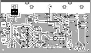
Veronica PCB and components layout
(View)
View full Circuit Diagram | Comments | Reading(2886)
Stereo Pll fm transmitter BH1417
Published:2012/10/10 1:48:00 Author:muriel | Keyword: Stereo Pll, fm transmitter
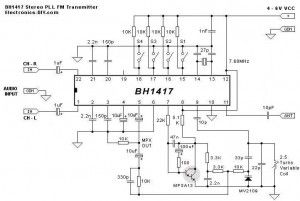
This BH1417 pll fm transmitter includes features like: pre-emphasis, sound limiter, stereo transmission, low pass filter, pll circuit, fm oscillator and rf output buffer. The sound limiter maintains the same audio level so no distorsions occur, the stereo encoder separates the left and right channel enabling stereo transmission, the low pass filter blocks any audio signal above 15 Khz to prevent rf interference and the pll circuit provides a rock solid frequency stability.There are 14 possible transmission frequencies with 200KHz increments selected with a 4-DIP switch. Starts from 88.7 up to 89.9 MHz and 107.7 up to 108.9 MHz.
Simply select transmission frequency at which you would like to transmit, set the combination for 4-DIP switch and BH1417 will tune to that frequency. If you can’t hear the transmitted audio signal on your FM receiver then re-adjust 2.5 turn variable coil until you can hear the signal.Technical Specifications:Supply Voltage: 4 – 6VTransmission Frequency: 87.7 – 88.9MHz, 106.7 – 107.9MHz (200kHz steps)Output RF Power: 20mWAudio Frequency: 20 – 15KHzSeparation: 40dBPower Consumption: 30mAComponents:1x BH1417 – Stereo PLL Transmitter IC (Case SOP22)1x 7.68 MHz Crystal1x MPSA13 – NPN Darlington Transistor1x 2.5 Turns Variable Coil1x MV2109 – Varicap Diode1x 4-DIP SwitchANT – 30 cm of copper wire
1x 22K Resistor7x 10K Resistor1x 5.1K Resistor2x 3.3K Resistor1x 100 Ohm Resistor 1x 100uF Capacitor3x 10uF Capacitor2x 1uF Capacitor
1x 47nF Capacitor3x 2.2nF Capacitor1x 1nF Capacitor1x 330pF Capacitor2x 150pF Capacitor1x 33pF Capacitor2x 27pF Capacitor1x 22pF Capacitor2x 10pF Capacitor
BH1417 Stereo pll transmitter circuit diagram
(View)
View full Circuit Diagram | Comments | Reading(1630)
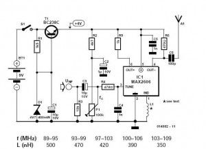
Mini FM Transmitter MAX2606
Published:2012/10/10 1:47:00 Author:muriel | Keyword: Mini, FM Transmitter
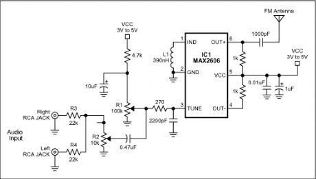
With MAX2606 we can make a small mono fm transmitter. It is build with MAX2606 and covers at least 20m with 1.5 m long copper wire antenna. You can use this transmitter as an oscillator but change the 1000pF capacitor from the antenna with 15pF.
MAX2606 transmitter output power is -10dBm, that means something around 100µW (micro-watts) = 0.0001W. Of course this is very low, that’s why we recommend you to use an auxiliary power amplifier if you want to build a more powerfull transmitter based on MAX2606. You can find a few fm power amplifiers on electroschematics.com so please use the search box.
Max2606 transmitter circuit diagram
(View)
View full Circuit Diagram | Comments | Reading(971)
Linear Optocoupler Circuit
Published:2012/10/9 2:35:00 Author:muriel | Keyword: Linear Optocoupler
This linear optocoupler is built with MOC5010 and can be used to isolate a circuit from main grid, audio interface, in medical electronics and many other applications. Because of its high isolation resistance (1011 Ω), MOC5010 is used in applications where a circuit is powered directly from main power. With a bandwidth from 5 Hz to 100 kHz you have no reason to complain about audio signal response.MOC5010 transforms an input current variation into an output voltage variation. The linear optocoupler circuit presented here has an amplification factor of 0.75. The input must not overcome 2 Vef while bandwidth is 118 kHz at -3 dB.Amplifier A has a transfer resistance of 200 mV/mA resulting in a total amplification of 0.6 … 0.8 (-4.5 … -2 dB). The output impedance is not higher than 200 Ω so you can connect an external amplifier at pin 4. If the input voltages are higher than 2 Vef then connect a potentiometer as voltage divider like showing below optocoupler circuit diagram.
Linear Optocoupler Circuit Diagram
If the global amplification is too small use a regular transistor instead of FET T1. It is important to mention that 2 separate power supplies are required: both the +12 V terminals as well the 0V (ground) must be isolated from one another. In many cases it is possible to use a 12V voltage for the transmitter part from the connected device. (View)
View full Circuit Diagram | Comments | Reading(1125)
Triangle Wave Generator circuit
Published:2012/10/9 2:35:00 Author:muriel | Keyword: Triangle, Wave Generator
This triangle wave generator is made with a trigger Schmitt that converts a triangle wave into a rectangular one used to charge and discharge a capacitor through current sources. The positive current source T1 provide the charging and T2 the discharging. The trigger Schmitt is made from OR-EXCL gates IC1a and IC1b.The rectangular signal amplitude must not be higher than the T1 and T2 base voltage. Assuming a 10 V power supply, results that the amplitude will be 2.5V. IC2 is a good quality operational amplifier (200 V/us) that acts like a buffer between Schmitt input and output.
The triangle wave generator circuit can generate signals with frequencies up to 300 kHz. With the component values presented in the diagram the output wave frequency is 38 kHz. The frequency can be adjusted by changing C1′s value. The wave generator assembly absorbs around 8 mA, of which 5 mA runs thru IC2.
Triangle Wave Generator Circuit Diagram
(View)
View full Circuit Diagram | Comments | Reading(1042)
Infrared Receiver circuit with BPW41N
Published:2012/10/9 2:35:00 Author:muriel | Keyword: Infrared Receiver circuit
This infrared receiver is used with this infrared transmitter. The output signal of D1 IR diode is amplified by IC1. The diode is BPW41N works great with the transmitter and is relatively fast (~200 ns). The impulses at IC1′s output are applied to IC2 (comparator) that separate them from ambient light. Check out the infrared alarm circuit too.The infrared received signal is decoded by a simple 2 divider, IC3a. Each impulse produces a change of the state at the stage output. The output signal is filtered with R7-C11 and decoupled with C12, resulting in an audio signal suitable for control of high impedance headphones.
Infrared Receiver Circuit Diagram
The output signal of the infrared receiver can be improved with the help of an order 3 active low-pass filter (cut freq at 10 – 12 kHz) that will serve as buffer stage too. With the receiver placed at 1 meter distance from the transmitter and 30% modulation, the signal to noise ratio is -50 dB. The maximum working distance without interferences was around 5 meters. The IR receiver circuit absorbs a current around 15 mA, this makes it advisable to use a rechargeable battery (NiCd). (View)
View full Circuit Diagram | Comments | Reading(833)
Impulse modulation infrared transmitter circuit
Published:2012/10/9 2:34:00 Author:muriel | Keyword: Impulse modulation, infrared transmitter
This infrared transmitter can be used with this infrared receiver. This transmitter uses. The modulated signal is produced by comparison of an audio signal with a triangle signal of high frequency using a comparator IC. An appropriate triangle signal generator must have the offset equal with half of the 5V power supply voltage and the triangular signal size is 2.5V. Check out the infrared alarm circuit too.For a wider range of the infrared transmitter the current through LEDs must he high. Because the LED cannot stand high dc currents, the impulses must be short so we use PWM. The pulses are generated by XOR gate IC2d that compares the original PWM signal with the delayed by R5-C3-IC2c. The IC2d output signal produce T1 switching and in this way the LEDs absorbed current is limited at 400 mA peak with help from R6. The average current consumption of the infrared transmitter circuit will be around 90 mA.
P3 adjustment is made without input signal with help of an oscilloscope, so that all impulses from the output signal have the same width. Then adjust P2 so that the intervals between impulses come equal. IC1 output will then be a perfect rectangular wave.
Working with the receiver and the transmitter at the same time feed an input signal at maximum value then adjust P1 to obtain minimum interference in the received signal. Finally, you may use IC2a and IC2b for the triangle signal generator.
Infrared Transmitter Circuit Diagram
(View)
View full Circuit Diagram | Comments | Reading(842)
Crystal Controlled 38 kHz IR Transmitter
Published:2012/10/8 2:35:00 Author:muriel | Keyword: Crystal,38 kHz, IR Transmitter
This is a precision 38 kHz Infrared transmitter using MOS integrated circuit uPD 6121.It uses the NEC transmission format ideally suited for remote operation in TV, VCD Player etc. The NEC transmission format includes leader codes, custom codes (16 bits), and data codes (16 bits).The frequency of oscillation is determined by the Crystal. The IR LEDs connected to the output emits IR pulses at 38kHz.The circuit is ideal for most IR Sensors since these are designed for 38 kHz pulsed IR rays. The circuit uses IC uPD6121. It is a CMOS version designed for IR transmission. It operates between 2 and 3.3 volts DC and maximum current consumption is 1 uA. It is a 20 pin IC.
Data codes of IC uPD 6121.
32 Codes single inputs, 3 Codes double inputs, expandable up to 64codes through SEL pin (pin7).Details of Pin connections are shown in the data sheet.
Crystal is connected between the OSCO (Pin8)and OSC1 (Pin9). Output drives a medium power NPN transistor T1 and the IR LEDs connected to its emitter gives pulsed IR rays
Crystal Controlled 38 kHz IR Transmitter Circuit
IC uPD 6121 Datasheet
IR Diodes and Crystal
(View)
View full Circuit Diagram | Comments | Reading(1095)
S / R ( set / reset ) pulse generator circuit ( integrated magnetic field sensor HMC1001/1002 )
Published:2012/10/7 21:39:00 Author:Ecco | Keyword: S / R , set , reset, pulse generator, integrated, magnetic field sensor
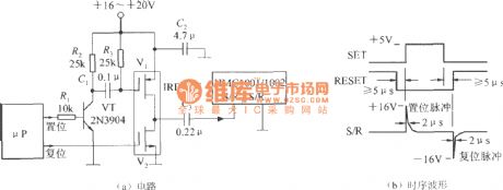
S / R pulse is set / reset pulse, of which amplitude depends on the measurement sensitivity of the MR sensor. For example, Tesla meter is composed of HMC1001/1002, when the minimum measurable flux density is 50nT, the amplitude of pulse current is required not less than 3A; when the minimum measurable flux density is 10 nT, the pulse current amplitude is not less than 4A. The higher measurement sensitivity is, the higher pulse current amplitude is. The circuit uses a microprocessor circuit to generate the S / R pulse, and the circuit is shown as the figure. This circuit uses +16 ~ +20 V power supply, and the pulse current can be more than 4A.
(View)
View full Circuit Diagram | Comments | Reading(2853)
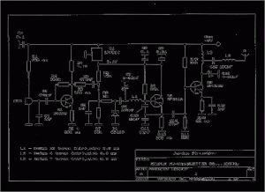
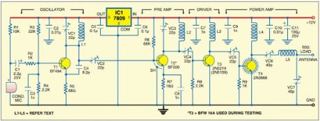
1 Watt Four Stage FM Transmitter
Published:2012/9/28 20:52:00 Author:muriel | Keyword: 1 Watt, Four Stage, FM Transmitter

This FM transmitter circuit uses four radio frequency stages: a VHF oscillator built around transistor BF494 (T1), a preamplifier built around transistor BF200 (T2), a driver built around transistor 2N2219 (T3) and a power amplifier built around transistor 2N3866 (T4). A condenser microphone is connected at the input of the oscillator. Working of the 1 Watt transmitter circuit is simple. When you speak near the microphone, frequency-modulated signals are obtained at the collector of oscillator transistor T1.
The FM signals are amplified by the VHF preamplifier and the pre-driver stage. You can also use transistor 2N5109 in place of 2N2219. The preamplifier is a tuned class-A RF amplifier and the driver is a class-C amplifier. Signals are finally fed to the class-C RF power amplifier, which delivers RF power to a 50-ohm horizontal dipole or ground plane antenna.
Use a heat-sink with transistor 2N3866 for heat dissipation (Note: or 2N4427 because it works better at 12 V and delivers up to 1 watt RF power). Carefully adjust trimmer VC1 connected across L1 to generate frequency within 88-108 MHz. Also adjust trimmers VC2 through VC7 to get maximum output at maximum range.
Regulator IC 78C09 provides stable 9V supply to the oscillator, so variation in the supply voltage will not affect the frequency generated. You can also use a 12V battery to power the circuit. Assemble the circuit on a general purpose PCB. Install the antenna properly for maximum range.
Coils L1 through L5 are made with 20 SWG copper-enamelled wire wound over air-cores having 8mm diameter. They have 4, 6, 6, 5 and 7 turns of wire, respectively.
Source: Electronics For You Magazine http://www.electronicsforu.com/electronicsforu/lab/freecircuitslist.asp?id=464&title=Four-Stage%20FM%20Transmitter
Note: This transmitter is meant only for educational purposes. use of this transmitter with outdoor antenna is illegal in most parts of the world.
FM Transmitter circuit diagram
(View)
View full Circuit Diagram | Comments | Reading(1355)
FSK Filter circuit
Published:2012/9/27 21:35:00 Author:muriel | Keyword: FSK Filter
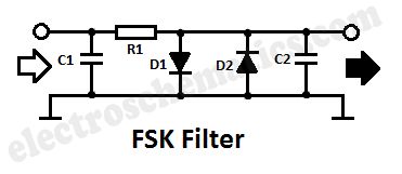
FSK or Frequency-Shift Keying is a form of frequency modulation in which the modulating signal shifts the output freq. between predetermined values. If problems arise in demodulating FSK signals, it is helpful to use the FSK filter circuit presented here. The Frequency-Shift Keying filter is very simple and it can be built inside a phone plug. The diagram shows a low pass filter made of R1 and C2. This filter has a cutoff freq. of about 1.6 KHz. Since the “0″ and “1″ signals of the FSK are sent as tones of 1.2 KHz and 2.4 KHz respectively, the filter removes all unwanted corners fron the signal.
Both D1 and D2 ensure that the FSK signal is limited to about +/- 600 mV amplitude. It can be attached to a loudspeaker or headphone output.
FSK Filter circuit diagram
Components valuesC1 = 0.0082C2 = 0.018R1 = 5.6kΩD1 = D2 = 1N4148 (View)
View full Circuit Diagram | Comments | Reading(1530)
Sync Signal Separator
Published:2012/9/27 21:31:00 Author:muriel | Keyword: Sync Signal, Separator
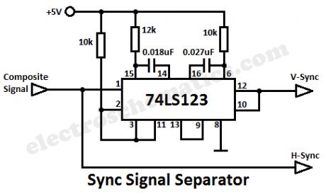
This simple sync signal separator circuit separates the composite sync signal into 2 separate horizontal and vertical sync signals.The composite signal can be directly used to drive the monitor’s horizontal sync input. That is why the composite signal line is connected directly to the H-sync line. To get the vertical sync signal, the double monoflop 74LS123 is needed as shown in the circuit diagram. The first monoflop time is somewhat longer than the distance between two line scan pulses. All horizontal line sync pulses are supressed. The second monoflop delivers only vertical sync pulses.
Sync Signal Separator circuit digram
(View)
View full Circuit Diagram | Comments | Reading(2438)
PWM Inverter
Published:2012/9/27 21:28:00 Author:muriel | Keyword: PWM Inverter
Pulse Width Modulation or PWM technology is used in Inverters to give a steady output voltage of 230 or 110 V AC irrespective of the load. The Inverters based on the PWM technology are more superior to the conventional inverters. The use of MOSFETs in the output stage and the PWM technology makes these inverters ideal for all types of loads. In addition to the pulse width modulation, the PWM Inverters have additional circuits for protection and voltage control.The quality of the output wave form (230 / 110 volt AC) from the inverter determines its efficiency. The quality of the inverter output wave form is expressed using Fourier analysis data to calculate the ‘Total Harmonic Distortion’ (THD). THD is the square root of the sum of the squares of the harmonic voltage divided by the fundamental voltage.
THD = √ V2 2 + V3 2 + V4 2…………. Vn 2 / V1Based on the output waveforms, there are three types of Inverters. These are Sine wave, Modified Sine wave or Quasi sine wave and Square wave inverters.
Sine waveAlternating current has continuously varying voltage, which swings from positive to negative. This has an advantage in power transmission over long distance. Power from the Grid is carefully regulated to get a pure sine wave and also the sine wave radiate the least amount of radio power during long distance transmission. But it is expensive to generate sine wave in an inverter. Its quality is excellent and almost all electrical and electronic appliances work well in sine wave inverter.
Sine Wave
The sine wave is the AC waveform we get from the domestic lines and from the generator. The major advantage of sine wave inverter is that all of the house hold appliances are designed to operate in sine wave AC. Another advantage is that the sine wave is a form of soft temporal rise voltage and it lacks harmonic oscillations which can cause unwanted counter forces on engines, interference on radio equipments and surge current on condensers.
Modified Sine wave or Quasi Sine wave
Modified sine wave is designed to simulate a sine wave since the generation of sine wave is expensive. This waveform consists of a Flat Plateau of positive voltage, dropping abruptly to zero for a short period, then dropping again to a flat plateau of negative voltage. It then go back to zero again and returning to positive. This short pause at zero volts gives more power to 50 Hz fundamental frequency of AC than the simple square wave.
(View)
View full Circuit Diagram | Comments | Reading(1218)
Best of FM Transmitter circuits
Published:2012/9/27 21:25:00 Author:muriel | Keyword: FM Transmitter
Here are some DIY FM Transmitter circuits that we have been published on electroschematics.com. This do-it-yourself fm transmitters are pretty easy to build and will give you a good feeling when you’ll hear the music on the radio receiver.Don’t forget to write your comments and post some links if you know good designs that are not in the best of list.
Best of Do-it-yourself FM Transmitters
1W FM Transmitter with 4 transistors
This FM transmitter circuit uses four radio frequency stages: a VHF oscillator built around transistor BF494 (T1), a preamplifier built around transistor BF200 (T2), a driver built around transistor 2N2219 (T3) and a power amplifier built around transistor 2N3866 (T4).
FM transmitter with MAX2606
Maxim now has available a series of five integrated oscillator building blocks in the MAX260x series which cover the frequency range between 45 and 650 MHz. The MAX2606 covers the VHF band, although the frequency can only be varied by approximately ±3 MHz around the midrange frequency set by the coil L.
SMD FM Transmitter
Let’s construct a low-power FM transmitter using surface-mount devices (SMD) that will be received with a standard FM radio. Soldering surface mounted devices is not so hard and actually is quite easy. The figure below shows the schematic of the transmitter which consists of two stages: an oscillator and an output amplifier. Modulation is from an electret microphone but you can use a low power audio source.
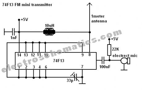
FM Bug Transmitter
Take a look at this fm spy transmitter which can be used as a bug transmitter or as fm bug too. It uses a single IC 74F13, one coil, a capacitor, one trimmer, one resistor and ofcourse one electret mic. This spy bug is so easy to build and can give you a total coverage range of about 3 to 5 meters. You may want to use a small 100mW amplifier to give a little extend transmission range so you can spy from other location.
(View)
View full Circuit Diagram | Comments | Reading(4477)
50 Hz Pulse Generator circuit
Published:2012/9/26 21:37:00 Author:muriel | Keyword: 50 Hz, Pulse Generator
Here is a Crystal based pulse generator that gives 50Hz clock pulses from its output. This circuit can be used as the front end of circuits that require precision 50Hz pulses.The circuit uses two counter ICs CD4060 and CD 4017 to divide the basic frequency to generate 50 Hz pulses. CD4060 is the ripple free binary counter IC and its basic frequency is controlled by a crystal connected in its pin 10 and 11. A 4.9152 MHz crystal is used in the circuit to generate clock pulses. CD4060 divides the 4.9152 crystal frequency by 16,384 so that from the Q13 (output pin 3) 300 Hz clock pulses available.
These clock pulses are then fed into the clock input pin14 of CD4017. It is the Johnson decade counter that divides the 300Hz pulses into 50 Hz pulses which are available from its Q5 (pin1) output.
50Hz Pulse Generator Circuit Diagram
(View)
View full Circuit Diagram | Comments | Reading(1274)
FM Radio Receiver circuit
Published:2012/9/26 21:35:00 Author:muriel | Keyword: FM, Radio Receiver
This simple fm radio receiver circuit consists of a regenerative rf stage, TR1, followed by a two of three-stage audio amplifier, TR2 to TR4. In some areas 3 stages of audio amplification may not be necessary, in which case TR3 and its associated components can be omitted and the free end of capacitor C5 connected to the collector of TR2. The critical part of the fm radio receiver is the first stage, TR1/VC1, where the wirings must be kept as short as possible. Coil L1 is formed by winding 8 turns of 1mm (20 swg) enamelled copper wire on a 6 mm diameter former, which is then removed. After that L1 should be stretched carefully and evenly to a length of about 13mm.
FM Radio Circuit Diagram
Transistors ListTR1 = BF199TR2 = TR3 = TR4 = BC547
Video presentation and photos of the working receiver
by Aleksandar
(View)
View full Circuit Diagram | Comments | Reading(952)
| Pages:36/195 At 202122232425262728293031323334353637383940Under 20 |
Circuit Categories
power supply circuit
Amplifier Circuit
Basic Circuit
LED and Light Circuit
Sensor Circuit
Signal Processing
Electrical Equipment Circuit
Control Circuit
Remote Control Circuit
A/D-D/A Converter Circuit
Audio Circuit
Measuring and Test Circuit
Communication Circuit
Computer-Related Circuit
555 Circuit
Automotive Circuit
Repairing Circuit