
Amplifier Circuit
Index 23
The amplifier board
Published:2013/1/16 2:12:00 Author:muriel | Keyword: amplifier board
View full Circuit Diagram | Comments | Reading(950)
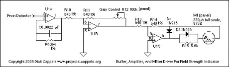
Output Amplifier
Published:2013/1/16 2:08:00 Author:muriel | Keyword: Output Amplifier
View full Circuit Diagram | Comments | Reading(740)
Input coupling and Preamp
Published:2013/1/16 2:07:00 Author:muriel | Keyword: Input coupling , Preamp
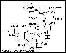
View full Circuit Diagram | Comments | Reading(712)
LM6172 voltage feedback amplifier and its pin main characteristics
Published:2013/1/16 1:14:00 Author:Ecco | Keyword: voltage feedback amplifier , pin main characteristics
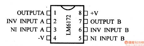
Operating voltage range is ± 5.0 to ± 15V; unity gain bandwidth is 110MHz; conversion rate is 3000V/μs; supply current is 4.6mA; Output Current is 50mA / channel; Input Offset Voltage is 0.4mA; input bias current is 1.2μA; common-mode input resistance is 40MΩ; differential input resistance is 4.9MΩ; PSRR = 95dB ; CMRR = 110dB.
(View)
View full Circuit Diagram | Comments | Reading(1009)
LM6181 current feedback amplifier and its pin main characteristics
Published:2013/1/16 1:32:00 Author:Ecco | Keyword: current feedback amplifier , pin main characteristics
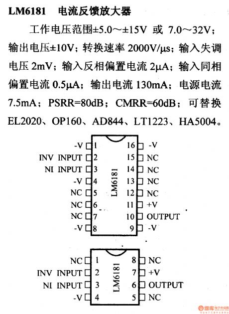
Operating voltage range is ± 5.0 ~ ± 15V or 7 ~~ 32V; output voltage is ± 10V; conversion rate is 2000mV/μs; input offset voltage is 2mV; reversed input bias current is 2μA; input in-phase bias current is 0.5μA; Output Current is 130mA; power current is 7.5mA; PSRR = 80dB; CMRR = 60dB; it can replace EL2020, OP160, AD844, LT1223 and HA5004.
(View)
View full Circuit Diagram | Comments | Reading(990)
MA337 JFET input op amp and its pin main characteristics
Published:2013/1/16 1:35:00 Author:Ecco | Keyword: JFET input, op amp , pin main characteristics

The input offset voltage is 100μV; noise is 8nV / √ ¯ Hz ( 1kHz); conversion rate is 15V/μs; power supply is ± 36V; differential-mode input voltage is ± 36V, the power consumption is 500mW.
(View)
View full Circuit Diagram | Comments | Reading(719)
MC13060 power amplifier and its pin main characteristics
Published:2013/1/16 1:01:00 Author:Ecco | Keyword: power amplifier , pin main characteristics
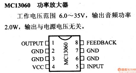
The operating voltage range is 6.0 ~ 35V, and the output audio power is 2.0W, and there is no relationship between output and power supply voltage.
(View)
View full Circuit Diagram | Comments | Reading(738)
MC4558 dual general - purpose operational amplifier and its pin main characteristics
Published:2013/1/16 1:07:00 Author:Ecco | Keyword: dual , general - purpose , operational amplifier , pin main characteristics
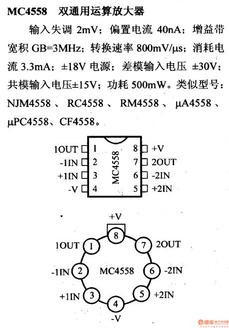
Input offset is 2mV; bias current is 40nA; Gain Bandwidth Product GB = 3MHz; conversion rate is 800mV/μs; Current consumption is 3.3mA; power supply is ± 18V; differential-mode input voltage is± 30V; common-mode input voltage is ± 15V; power consumption is 500mW. Similar models: NJM4558, RC4558, RM4558, μA4558, μPC4558 and CF4558.
(View)
View full Circuit Diagram | Comments | Reading(1167)
MC1445/1545 broadband amplifier and its pin main characteristics
Published:2013/1/15 1:22:00 Author:Ecco | Keyword: broadband amplifier, pin main characteristics
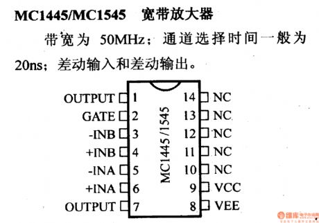
Broadband is 50MHz; channel selection time is typically 20ns; it has differential input and differential output.
(View)
View full Circuit Diagram | Comments | Reading(1293)
MC1733CB differential video amplifier and its pin main characteristics
Published:2013/1/15 1:57:00 Author:Ecco | Keyword: differential video amplifier , pin main characteristics

It has a differential input and differential output, and the gain is fixed in 10V, 100V and 400V when it has no external devices. It can use an external resistor to adjust gain in the range of10V ~ 400V; Bandwidth is 120MHz; rise time is 2.5ns; delay time is 3.6ns.
(View)
View full Circuit Diagram | Comments | Reading(782)
MC1748C operational amplifier and its pin main characteristics
Published:2013/1/15 1:50:00 Author:Ecco | Keyword: operational amplifier, pin main characteristics
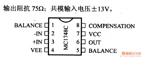
It has short circuit protection; the MC1741 has no compensation; CMRR = 90dB; when it has unity gain, it just needs a 30pF compensation capacitor; working power is ± 15V; PSRR is greater than 75dB; output impedance is 75Ω; common-mode input voltage is ± 13V.
(View)
View full Circuit Diagram | Comments | Reading(716)
MC3458 dual and single- supply op amp and its pin main characteristic
Published:2013/1/15 1:44:00 Author:Ecco | Keyword: dual , single- supply , op amp , pin main characteristic
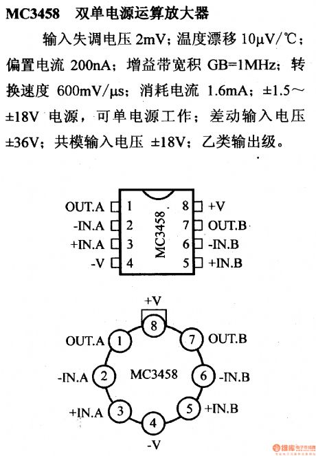
2mV input offset voltage; 10 μV / ℃ temperature drift; 200nA bias current; Gain Bandwidth Product GB = 1MHz; 600mV/μs conversion rate; 1.6mA Current consumption; ± 1.5 to ± 18V power supply, and it can be a single -supply operation; differential input voltage is ± 36V; common-mode input voltage is ± 18V; Group B output stage.
(View)
View full Circuit Diagram | Comments | Reading(1201)
NE531 high - speed operational amplifier and its pin main characteristics
Published:2013/1/15 1:36:00 Author:Ecco | Keyword: high - speed , operational amplifier , pin main characteristics
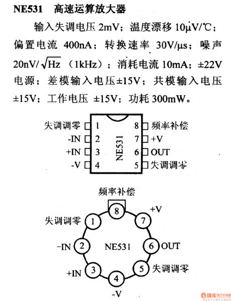
2mV input offset voltage; 10 μV / ℃ temperature drift; 400nA bias current; 30V/μs conversion rate; 20nV / √ ¯ Hz (1Hz) noise; 10mA Current consumption; ± 22V power supply; ± 15V differential-mode input voltage; ± 15V common-mode input voltage; 300mW power consumption.
(View)
View full Circuit Diagram | Comments | Reading(1066)
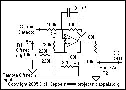
The Preamp
Published:2013/1/15 0:53:00 Author:muriel | Keyword: The Preamp
View full Circuit Diagram | Comments | Reading(828)
Photocell Amplifier
Published:2013/1/15 0:29:00 Author:muriel | Keyword: Photocell Amplifier
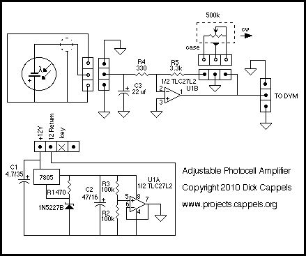
View full Circuit Diagram | Comments | Reading(944)
NJM4560 dual wideband op amp and its pin main characteristics
Published:2013/1/11 1:45:00 Author:Ecco | Keyword: dual wideband op amp , pin main characteristics
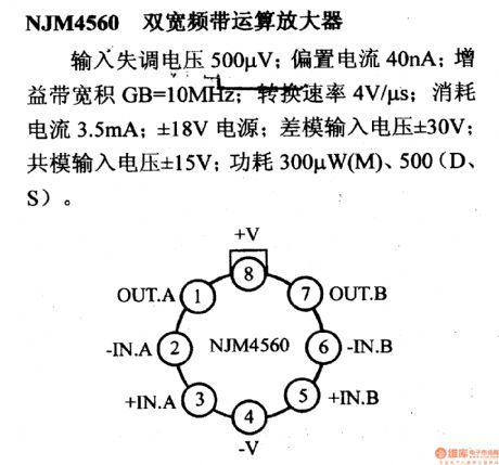
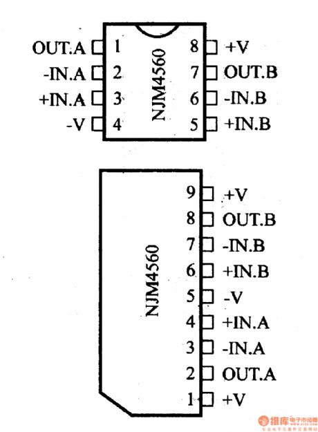
500μV input offset voltage; 40nA bias current; Gain Bandwidth Product GB = 10MHz; 4V/μs conversion rate; 3.5mA current consumption; ± 18V power supply; ± 30V differential-mode input voltage; ± 15V common-mode input voltage; power is 300μW ( M),or 500μW (D, S).
(View)
View full Circuit Diagram | Comments | Reading(3507)
NJM4562 dual low-noise op amp and its pin main characteristics
Published:2013/1/11 1:56:00 Author:Ecco | Keyword: dual low-noise op amp , pin main characteristics
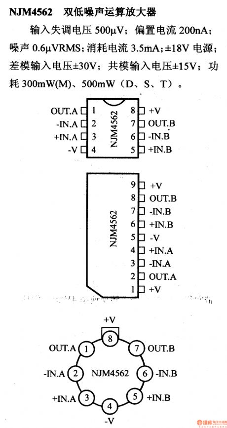
500μV input offset voltage; 200nA bias current; 4V/μs conversion rate; 0.6μVRMS noise; 3.5mA current consumption; ± 18V power supply; ± 30V differential-mode input voltage; ± 15V common-mode input voltage; power is 300μW ( M),or 500μW (D, S, T).
(View)
View full Circuit Diagram | Comments | Reading(1138)
OP-06 high-gain operational amplifier and its pin main characteristics
Published:2013/1/11 2:03:00 Author:Ecco | Keyword: high-gain, operational amplifier , pin main characteristics
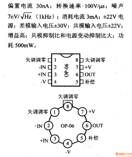
60μV input offset voltage; 300nV / ℃ temperature drift; 30nA bias current; 100V/μs conversion rate; 7nV / √ ¯ Hz (1Hz ) noise; 3mA current consumption; ± 22V power supply; ± 30V differential-mode input voltage; ± 22V common-mode input voltage; the gain is high; common-mode rejection ratio and power supply rejection ratio are large; the power consumption is 500mW.
(View)
View full Circuit Diagram | Comments | Reading(711)
OP-07 Low offset operational amplifier and its pin main characteristics
Published:2013/1/11 2:28:00 Author:Ecco | Keyword: Low offset , operational amplifier, pin main characteristics

Input offset voltage is 10μV; temperature drift is 200nV / ℃; bias current is 700pA; Gain Bandwidth Product GB = 600kHz; conversion rate is 300mV/μs; the noise is 9.6nV / √ ¯ Hz (1Hz ); Current consumption is 2.5mA ; power supply is ± 22V; differential mode input voltage is ± 30V; common-mode input voltage is ± 22V ; the power is 500mW.
(View)
View full Circuit Diagram | Comments | Reading(923)
OP-37 wide-band high-precision, high - speed operational amplifier and its pin main characteristics
Published:2013/1/11 2:36:00 Author:Ecco | Keyword: wide-band , high-precision, high - speed , operational amplifier, pin main characteristics
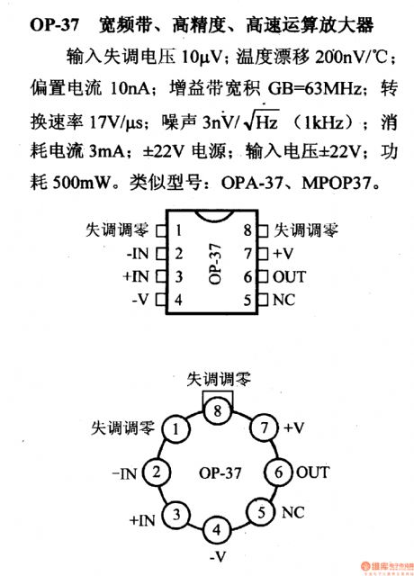
Input offset voltage is 10 μV; temperature drift is 200nV / ℃; bias current is 10nA; Gain Bandwidth Product GB = 63kHz; conversion rate is 17V/μs; noise is 3nV / √ ¯ Hz (1Hz ); Current consumption is 3mA; input voltage is ± 22V; power supply is ±22V; power consumption is 500mW. Similar models: OPA- 37, MPOP37.
(View)
View full Circuit Diagram | Comments | Reading(748)
| Pages:23/250 At 202122232425262728293031323334353637383940Under 20 |
Circuit Categories
power supply circuit
Amplifier Circuit
Basic Circuit
LED and Light Circuit
Sensor Circuit
Signal Processing
Electrical Equipment Circuit
Control Circuit
Remote Control Circuit
A/D-D/A Converter Circuit
Audio Circuit
Measuring and Test Circuit
Communication Circuit
Computer-Related Circuit
555 Circuit
Automotive Circuit
Repairing Circuit