
Amplifier Circuit
Index 24
1.3W Power Amplifier
Published:2013/1/10 21:42:00 Author:muriel | Keyword: 1.3W, Power Amplifier
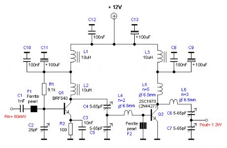
View full Circuit Diagram | Comments | Reading(1097)
INA110 high precision JFET input instrumentation amplifier and its pin main characteristics
Published:2013/1/10 3:01:00 Author:Ecco | Keyword: high precision , JFET input, instrumentation amplifier , pin main characteristics
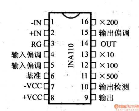
The maximum operating voltage is ± 18V; input voltage range is ± VCC; bias current is less than 50pA; stabilizing time is less than 4μs; common-mode rejection ratio is 106dB; gain can be 1,10,100,200 and 500, and it is convenient to convert; temperature drift voltage is less than 2mV / ℃, pin is compatible with the AD524, AD624.
(View)
View full Circuit Diagram | Comments | Reading(1330)
ISO100 broadband isolation amplifier and its pin main characteristics
Published:2013/1/10 2:46:00 Author:Ecco | Keyword: broadband isolation amplifier , pin main characteristics
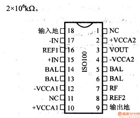
The maximum operating voltage is ± 18V; isolation voltage is 2500V; input current range is ± 1mA (Vout / in = RF); leakage current is less than 0.3μA; bandwidth is 60kHz; the total analog rejection ratio CMRR = 90dB; common-mode input voltage is ± 10V; output impedance is 2000000kΩ.
(View)
View full Circuit Diagram | Comments | Reading(975)
ISO106 high pressure isolation buffer amplifier and its pin main characteristics
Published:2013/1/10 2:41:00 Author:Ecco | Keyword: high pressure , isolation buffer amplifier , pin main characteristics
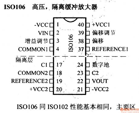
ISO106's performance is same with ISO102, and the main difference has the following two points: 1.ISO106 continuous isolation voltage is 3500V; 2.ISO106 uses 40 -pin DIP package; and the major pin definitions can be found in the ISO102.
(View)
View full Circuit Diagram | Comments | Reading(801)
LM6182 current feedback amplifier and its pin main characteristics
Published:2013/1/10 2:37:00 Author:Ecco | Keyword: current feedback amplifier, pin main characteristics
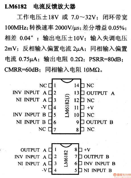
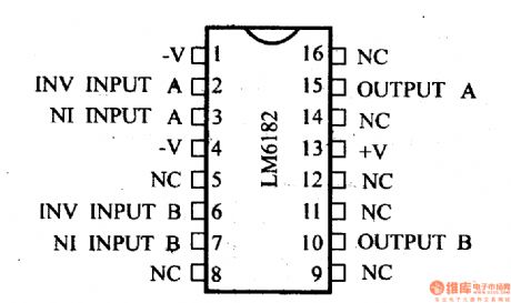
Operating voltage range is ± 18V or 7.0 ~32V; closed-loop bandwidth is 100MHz; conversion rate is 2000V/μs; differential gain is 0.05%; difference is 0.04 °; output voltage is ± 10V; input offset voltage is 2mV; inverting input bias current is 2μA; noninverting input bias current is 0.75μA; output resistance is 0.2Ω; PSRR = 80dB; CMRR = 60dB; noninverting input resistance is 10MΩ.
(View)
View full Circuit Diagram | Comments | Reading(831)
Dual operational amplifier and its pin main characteristics
Published:2013/1/10 2:14:00 Author:Ecco | Keyword: Dual operational amplifier, pin main characteristics
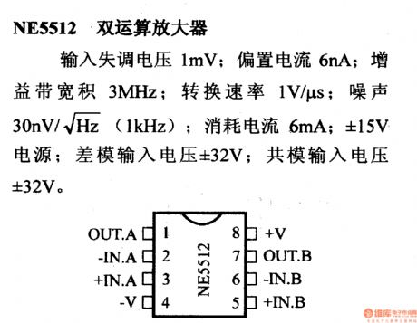
Input offset voltage is 1mV; bias current is 6nA; Gain Bandwidth Product GB = 3MHz; conversion rate is 1V/μs; noise is 30nV / √ ¯ Hz ( 1kHz); Current consumption is 6mA ; power supply is ± 15V; differential-mode input voltage is ± 32V; common mode input voltage is ± 32V.
(View)
View full Circuit Diagram | Comments | Reading(876)
LM7171 voltage feedback amplifier and its pin main characteristics
Published:2013/1/9 1:41:00 Author:Ecco | Keyword: voltage feedback amplifier , pin main characteristics
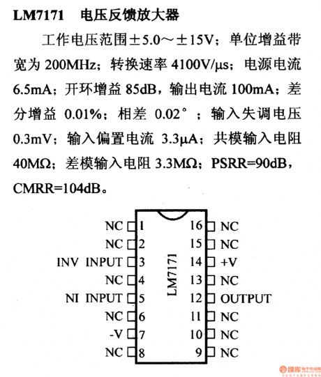
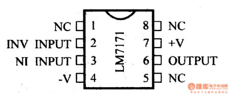
Operating voltage range is ± 5.0 to ± 15V; conversion rate is 4100V/μs; unit gain bandwidth is 200MHz; supply current is 6.5mA; input offset voltage is 0.3mV; input bias current is 3.3μA; PSRR = 90dB , CMRR, = 107dB; common-mode input resistance is 40MΩ; differential input resistance is 3.3MΩ; open -loop gain is 85dB; 100mA output current; differential gain is 0.01%; difference is 0.02 °.
(View)
View full Circuit Diagram | Comments | Reading(1893)
LM7121 voltage feedback amplifier and its pin main characteristics
Published:2013/1/9 1:36:00 Author:Ecco | Keyword: voltage feedback amplifier and its pin main characteristics
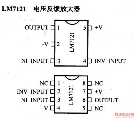
Operating voltage range is ± 5.0 to ± 15V or a single 5.0 ~ 36V; conversion rate is 1300V/μs; unity gain bandwidth is 175MHz; supply current is 5.3mA; input offset voltage is 0.9mV; input bias current is 5.2μA; - PSRR = 81dB CMRR = 93dB, + PSRR = 86dB; common-mode input resistance is 10MΩ; differential input resistance is 3.4MΩ.
(View)
View full Circuit Diagram | Comments | Reading(901)
LM6171 voltage feedback amplifier and its pin main characteristics
Published:2013/1/9 0:31:00 Author:Ecco | Keyword: voltage feedback amplifier , pin main characteristics
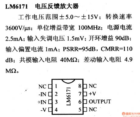
Operating voltage range is ± 5.0 to ± 15V; conversion rate is 3600V/μs; unity gain bandwidth is 100MHz; supply current is 2.5mA; input offset voltage is 1.5mV; open loop gain is 90dB; input bias current is 1mA; PSRR = 95dB, CMRR, = 110dB; common mode input resistance is 40M; differential input resistance is 4.9MΩ.
(View)
View full Circuit Diagram | Comments | Reading(1070)
Double low-drift JFET input op amp and its pin main characteristic
Published:2013/1/9 0:23:00 Author:Ecco | Keyword: Double, low-drift, JFET input , op amp , pin main characteristic
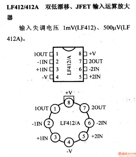
The input offset voltage is 1mV(LF412), 500μV(LF412A).
(View)
View full Circuit Diagram | Comments | Reading(814)
OP-16 JFET input op amp and its pin main characteristics
Published:2013/1/8 1:10:00 Author:Ecco | Keyword: JFET , input op amp , pin main characteristics
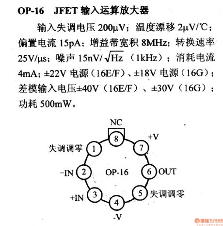
200μV input offset voltage; 2μV / ℃ temperature drift; 15pA bias current; gain-bandwidth product GB= 8MHz; 25V/μs conversion rate; 15nV / √ ¯ Hz ( 1kHz) noise; 4mA consumption current; ± 22V power supply (16E / F ), ± 18V power supply (16G); ± 40V (16E / F) , ± 30V (16G )differential-mode input voltage.
(View)
View full Circuit Diagram | Comments | Reading(1022)
OP-20 high-precision operational amplifier and its pin main characteristics
Published:2013/1/8 1:16:00 Author:Ecco | Keyword: high-precision, operational amplifier, pin main characteristics
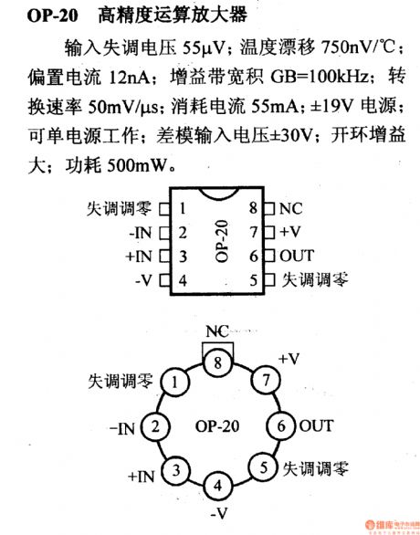
55μV input offset voltage; 750nV / ℃ temperature drift; 12nA bias current; Gain Bandwidth Product GB = 100kHz; 50mV/μs conversion rate; 55mA current consumption; power supply is ± 19V, and it can use a single -supply operation; ± 30V differential-mode input voltage; open loop gain is high; power consumption is 500mW.
(View)
View full Circuit Diagram | Comments | Reading(699)
OP-21 high-precision operational amplifier and its pin main characteristics
Published:2013/1/8 1:20:00 Author:Ecco | Keyword: high-precision , operational amplifier , pin main characteristics
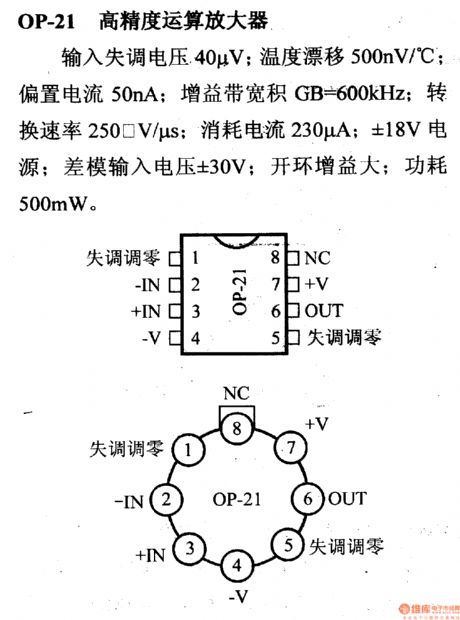
The input offset voltage is 40μV; temperature drift is 500nV / ℃; bias current is 50nA; Gain Bandwidth Product GB = 600kHz; Current consumption is 230μA; power supply is ± 18V; differential-mode input voltage is ± 30V; open-loop gain is high, the power consumption is 500mW.
(View)
View full Circuit Diagram | Comments | Reading(721)
OP-22 programmable op amp and its pin main characteristics
Published:2013/1/8 0:58:00 Author:Ecco | Keyword: programmable op amp , pin main characteristics
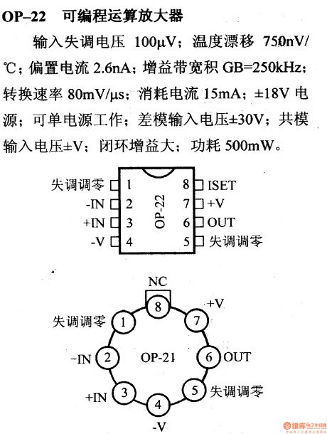
Input offset voltage is 100μV; temperature drift is 750nV / ℃; bias current is 2.6nA; Gain Bandwidth Product GB = 250kHz; conversion rate is 80mV/μs; Current consumption is 15mA ; ± 18V power supply; it can be a single -supply operation; differential-mode input voltage is ± 30V; the common-mode input voltage is ± V; closed-loop gain is high; power consumption is 500mW.
(View)
View full Circuit Diagram | Comments | Reading(871)
OP-27 ultra-low noise and high - precision operational amplifier and its pin main characteristics
Published:2013/1/8 0:53:00 Author:Ecco | Keyword: ultra-low noise , high - precision , operational amplifier , pin main characteristics
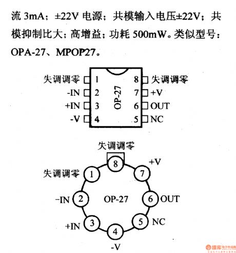
Input offset voltage is 10 μV ; the temperature drift is 200nV / ℃; bias current is 10nA; gain-bandwidth product GB= 8MHz ; conversion rate is 2.8V/μs; noise is 3mV / √ ˉ Hz (1kHz); Current consumption is 3mA ; ± 22V power supply; common mode input voltage is ± 22V; CMRR is high; high gain; power consumption is 500mW. The similar models: OPA- 27 , MPOP27.
(View)
View full Circuit Diagram | Comments | Reading(1124)
MAX4100/MAX4101 high-speed operational amplifier and its pin main characteristics
Published:2013/1/7 1:25:00 Author:Ecco | Keyword: high-speed, operational amplifier , pin main characteristics
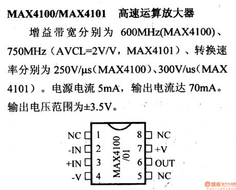
Gain bandwidth is 600MHz (MAX4100), 750MHz (AVCL=2V/V,MAX4101). The conversion rates are respectively 250V/μ s (MAX4100) and 300V/μ s (MAX4101). Output current is 70mA. Output voltage range is ±3.5V.
(View)
View full Circuit Diagram | Comments | Reading(851)
MAX4106/MAX4107 high-speed operational amplifier and its pin main characteristics
Published:2013/1/7 1:22:00 Author:Ecco | Keyword: high-speed , operational amplifier, pin main characteristics
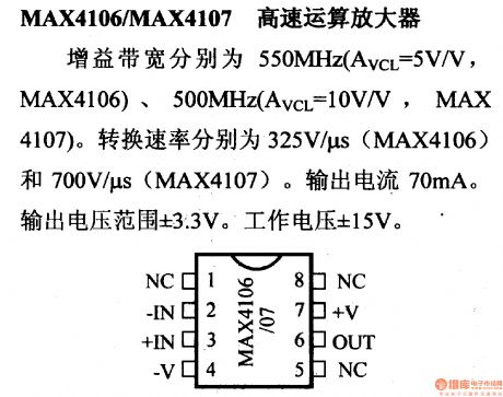
Gain bandwidth is 550MHz (AVCL=5V/V,MAX4106), 500MHz (AVCL=10V/V,MAX4107). The conversion rates are respectively 325V/μ s (MAX4106) and 700V/μ s (MAX4107). Output current is 70mA. output voltage range is ±3.3V. Working voltage is ± 15V.
(View)
View full Circuit Diagram | Comments | Reading(760)
LM725 high-precision operational amplifier and its pin main characteristics
Published:2013/1/7 1:32:00 Author:Ecco | Keyword: high-precision , operational amplifier, pin main characteristics
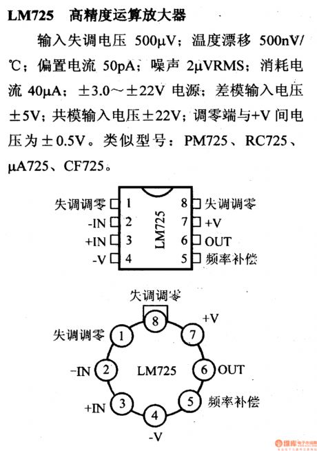
Input offset voltage is 500 μV; temperature drift is 500nV/℃; bias current is 50pA; noise is 2 μ VRMS; current consumption is 40 μA; power supply is ± 3.0~ ± 22V; differential mode input voltage is ± 5V; common-mode input voltage is ± 22V; the voltage between zero Terminal and +V is ± 0.5V. Similar models: PM725,RC725, Mu A725,CF725.
(View)
View full Circuit Diagram | Comments | Reading(1095)
MA345 dual low-power operational amplifier and its pin main characteristics
Published:2013/1/7 1:12:00 Author:Ecco | Keyword: dual , low-power , operational amplifier , pin main characteristics
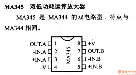
MA345 is the double circuits model of MA344. The characteristics are same with MA344.
(View)
View full Circuit Diagram | Comments | Reading(647)
LM7131 single supply operational amplifier and its pin main characteristics
Published:2013/1/7 1:38:00 Author:Ecco | Keyword: single supply , operational amplifier , pin main characteristics
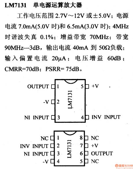
Operating voltage range is 2.7V ~ 12V or ± 5.0V; Supply Current is 7.0mA (5.0V ) and 6.5mA (3.0V ); the harmonic distortion is 0.1 % at 4MHz; Gain Bandwidth is 70MHz ; bandwidth is 90MHz-dB; output current is 40mA; input bias current is 20μA to 50Ω load; voltage gain is 60dB; CMRR = 70dB ; PSRR = 75dB.
(View)
View full Circuit Diagram | Comments | Reading(744)
| Pages:24/250 At 202122232425262728293031323334353637383940Under 20 |
Circuit Categories
power supply circuit
Amplifier Circuit
Basic Circuit
LED and Light Circuit
Sensor Circuit
Signal Processing
Electrical Equipment Circuit
Control Circuit
Remote Control Circuit
A/D-D/A Converter Circuit
Audio Circuit
Measuring and Test Circuit
Communication Circuit
Computer-Related Circuit
555 Circuit
Automotive Circuit
Repairing Circuit