
Time Control
Index
REACTION TIMER GAME
Published:2013/8/5 20:09:00 Author:lynne | Keyword: REACTION TIMER GAME
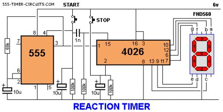
This is a game for two players. Player 1 presses the START button. This resets the 4026 counter chip and starts the 555 oscillator. The 555 produces 10 pulses per second and these are counted by the 4026 chip and displayed on the 7-Segment display. The second player is required to press the STOP button. This freezes the display by activating the Clock Inhibit line of the 4026 (pin 2).Two time-delay circuits are included. The first activates the 555 by charging a 10u electrolytic and at the same time delivering a (high) pulse to the 4026 chip to reset it. The second timer freezes the count on the display (by raising the voltage on pin 2) so it can be read.
(View)
View full Circuit Diagram | Comments | Reading(2669)
Adjustable Analog Timer
Published:2013/3/25 4:02:00 Author:Ecco | Keyword: Adjustable Analog Timer
This is a very simple adjustable analog timer circuit diagram. You can build this circuit just for fun, for newbie project or may be…, this circuit could be used to set a time limit when playing games or as an egg-timer in the kitchen.
(View)
View full Circuit Diagram | Comments | Reading(2402)
All-Ears QSK Timing Generator
Published:2013/3/7 3:10:00 Author:Ecco | Keyword: All-Ears, QSK, Timing Generator

In the world of amateur (ham) radio morse code communications, QSK refers to a method of operation where the transmitter and receiver are alternately active when the key is down or up. QSK is also known as break-in keying. QSK operation allows the operator to hear what is happening on their frequency in the brief times between transmitting morse code dits and dahs. The conversation can be quickly interrupted by the other station, or by a third station. The sender also knows immediately if their signal is being interfered with.
The design of a QSK-capable radio station is somewhat tricky. A QSK system has to quickly switch the antenna between the transmitter and receiver, key the transmitter, mute the receiver during transmission and disable the transmitter's oscillator during receiving. It is also desirable to change the receiver's AGC response time from fast to slow when not transmitting. By adding small delays at the beginning and ending of the dots and dashes, it is possible to generate signals with slightly longer and shorter lengths compared the original morse code. These modified signals sequence the entire system in order to eliminate transmitted chirps, T/R relay arcing and receiver clicking.
Here's a typical sequence for sending one morse code dit , items in parentheses happen simultaneously: (key down, T/R relay to transmit, transmitter oscillator on, receiver mute), delay, transmitter output on for duration of dit, (key up, transmitter output off), delay, (T/R relay to receive, transmitter oscillator off, receiver unmute) Additionally, the receiver AGC slow/fast signal needs to go to fast at the beginning the the first key down event, and should switch to fast a few seconds after the last key up event.
This circuit takes a TTL-level keying signal and produces three TTL-level output signals, and inverted versions of the three signals. This combination of outputs is useful for driving a variety of control circuits that can interface to the transmitter and receiver. The timing generator also generates the necessary signals for automatic non-QSK transmit/receive switching.
(View)
View full Circuit Diagram | Comments | Reading(1831)
SERVO TESTER Circuit
Published:2013/3/5 20:45:00 Author:Ecco | Keyword: SERVO TESTER
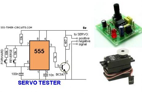
This circuit can be used to manually turn a servo clockwise and anti-clockwise. By pushing the forward or reverse button for a short period of time you can control the rotation of the servo. It will also test a servo. Here is a photo of a kit from Cana Kit for $10.00 plus postage (it is a slightly different circuit) and a motor and gearbox, commonly called a servo. The output shaft has a disk or wheel containing holes. A linkage or push-rod is fitted to a hole and when the disk rotates, the shaft is pushed and pulled. The shaft only rotates about 180?to actuate flaps or ailerons etc.
(View)
View full Circuit Diagram | Comments | Reading(6710)
NE555 Monostable
Published:2012/12/5 Author:muriel | Keyword: NE555 Monostable
View full Circuit Diagram | Comments | Reading(1038)
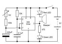
Adjustable Timer circuit 1-10 minute
Published:2012/9/25 21:47:00 Author:muriel | Keyword: Adjustable, Timer circuit, 1-10 minute
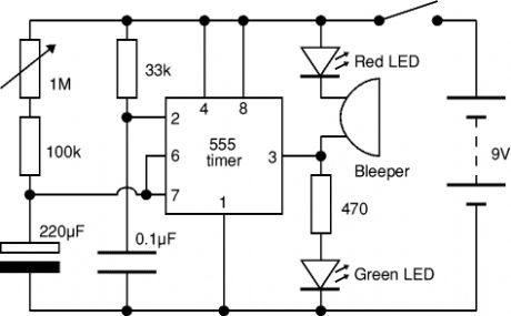
The Adjustable Timer circuit starts timing when switched on. The green LED lights to show that timing is in progress. When the time period is over the green LED turns off, the red LED turns on and the bleeper sounds. The time period is set by adjusting the variable resistor. It can be adjusted from 1 to 10 minutes (approximately) with the parts shown in the diagram. You can mark the times on a scale drawn on the box.Please note that the range of time periods is only approximate. With perfect components the maximum time period should be 4? minutes, but this is typically extended to about 10 minutes because the 220μF timing capacitor slowly leaks charge. This is a problem with all electrolytic capacitors, but some leak more than others. In addition the actual value of electrolytic capacitors can vary by as much as ±30% of their rated value.
Adjustable 10 minute timer schematic
(View)
View full Circuit Diagram | Comments | Reading(2028)
Delay circuit with NE555 timer
Published:2012/9/16 20:48:00 Author:Ecco | Keyword: Delay , timer
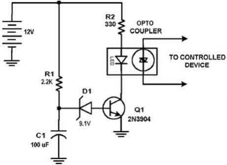
This circuit design was used to switch on device via a LED photocell arrangement (optocoupler) using components R1, C1, D1 and Q1. It produces a delay on powering up to ensure correct sequencing of certain equipment. A very simple delay timer using a single transistor and an R-C timing circuit.
(View)
View full Circuit Diagram | Comments | Reading(0)
0-60sec start-stop timer with 555
Published:2012/9/12 20:43:00 Author:Ecco | Keyword: 0-60sec, start-stop timer , 555
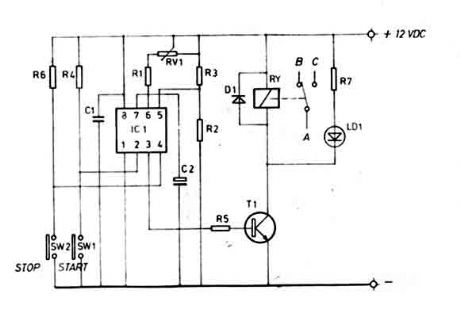
This timer is ideal for small aplications. Due to its simple structure, its usage and nevertheless its universal character, this mini timer is usable in the most current applications needing time intervals, from some seconds through approximately 60 minutes. By simple modifications it is possible to adjust the maximum time and the timing scale, as necessary. A strong output, made by a relay, permits to adapt, on the input and the output, whatever apparatus. (View)
View full Circuit Diagram | Comments | Reading(4108)
LONG PERIOD COMPUTER WATCH DOG TIMER
Published:2012/9/5 20:53:00 Author:Ecco | Keyword: LONG PERIOD, COMPUTER WATCH DOG, TIMER
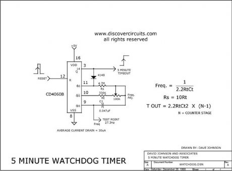
This circuit uses a simple 4060 IC oscillator/timer that is reset periodically by a computer. Should the computer fail to send a pulse, the output changes state. The time can easily be set from seconds to hours.
Source: discovercircuits (View)
View full Circuit Diagram | Comments | Reading(3083)
Touch Switch Monostable/Timer with 555 IC
Published:2012/9/3 2:45:00 Author:Ecco | Keyword: Touch Switch , Monostable, Timer , 555 IC
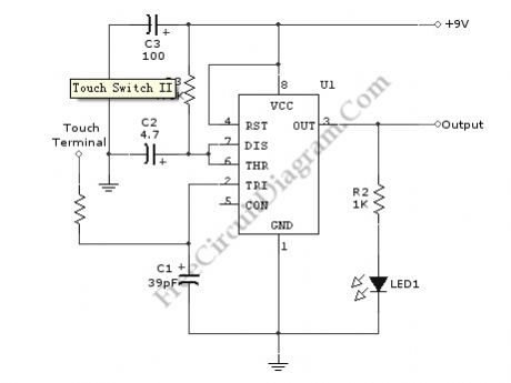
Using the given values as shown in the schematic diagram, this circuit has timed ON period of 4 seconds. The value of C2 and R3 determines the ON time, increasing the value of C2 or R3 will increase the ON time. The ON time is decreased if the value of C2 or R3 is decreased.
A schematic diagram of a touch switch circuit is shown below. This circuit consist of timer, one shoot multivibrator and touch terminal. As timer, this circuit uses 555 timer which is connected to one-shot multivibrator. The touch terminal is used to trigger this circuit. The output of this circuit can be used to drive a power transistor, CMOS circuitry, hexFET transistor or optocoupler. Here is the schematic diagram of the touch switch circuit: (Source: freecircuitdiagram)
(View)
View full Circuit Diagram | Comments | Reading(2725)
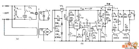
60h timing circuit
Published:2011/12/1 21:39:00 Author:May | Keyword: 60h timing
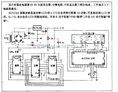
This timer consists of three parts: power supply double 50Hz square wave generator, frequency dividing circuit, timing display. Its working volt is 5V. Its current is several milliampere.
5G7224A is 4 1/2 bit fully decoded counter driving LCD. It is 60 system and it can direct-coupling LCD. D1~D5 state each bit LCD drive line group. Switch K is used for controlling time/suspend ; Switch AN is used for controlling zero clearing .
(View)
View full Circuit Diagram | Comments | Reading(1842)
Triple-digit display electronic timer circuit composed of NE555 and CD40110
Published:2011/8/30 1:58:00 Author:Jessie | Keyword: Triple-digit display , electronic timer
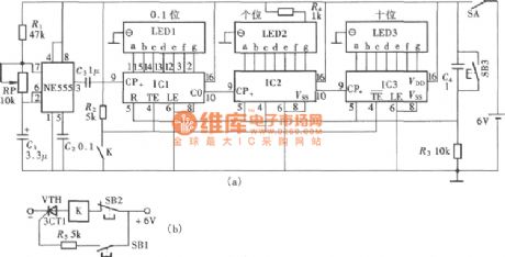
As shown in figure is electronic timing which is used for raider type cars. Car startups will launch timer,while car stops makes the timer stop.The value that car showsis the racing spending time. This circuit is composedof thecontrol switch and electronic timer. And electronic timerconsists of the time base generator and digital electronic counter. (A)is principle diagram; (b)is control switch circuit. IC1, IC2 and IC3are CD40110. (View)
View full Circuit Diagram | Comments | Reading(3530)
Countdown display timer circuit with NE556, CD40110
Published:2011/8/30 2:01:00 Author:Jessie | Keyword: Countdown display timer
Digital display countdown timer can make people always see how much time left, it has certain practical value to some applications. As shown in figure, itis a digital display timing circuit, its structure is simple, and is easy to make. Its time-base unit adjustable. This circuit uses harmonic oscillator, which is composedof NE555 circuit as time base. Although the time precision is not quite high, it is economical and suitable. Full circuitis composedof adjustable time base signal generator, minus count, display and output signal control circuit etc. (View)
View full Circuit Diagram | Comments | Reading(3909)
Open/stop selecting function timer circuit with CD4541
Published:2011/8/30 2:11:00 Author:Jessie | Keyword: Open/stop selecting function, timer
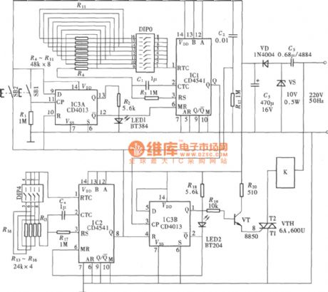
CD4541 is the main partof the timer. It can chooseto open firstly, or stopby switch. In circuit, timing time's adjustment is choosing by switch,the amount of the resistance between CD4541's pin1 and pin 2increasing and decreasing. Because resistance is decided as first, every resistoris fixed. So it is more convenient and accurate than the potentiometer to adjust timing time.The Circuit is composedofthe open/stop preset circuit, adjustable open/stop timing circuit, output control and executing circuit. (View)
View full Circuit Diagram | Comments | Reading(6141)
Circulation regularly reminded decoder circuit with CD4511
Published:2011/8/30 2:20:00 Author:Jessie | Keyword: Circulation regularly reminded decoder
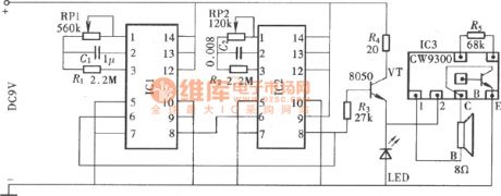
It uses two CD4541 connected in series to compose a circulation timer. The output terminal connected a sound circuitto form a regularly reminder circuit. This regularly reminder circuit has many uses, such as for the patient's care, regularly reminded medication, etc. Reminding sound circuit can be chosenaccording topeople's favoritemusic integrated circuit. This timer chooses musical CW9300 as sound circuit,and itscomposition is as shown. (View)
View full Circuit Diagram | Comments | Reading(2222)
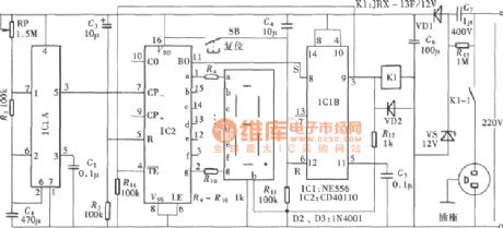
Electrical apparatus start-stop circulatory timer circuit diagram
Published:2011/10/20 21:40:00 Author:Rebekka | Keyword: Electrical apparatus , start-stop circulatory timer
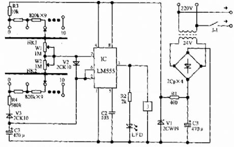
LM555 integrated circuit forms the basic duty cycle adjustable multivibrator. Discharge and charge circuit of C3 are connected to KH1, W1, KH2, W2 respectively in series for coarse tuning, fine-tuning the stop time. When the circuit starts to work, the power supply passes R3, HK1 series resistor and W1, V2 to C3, thenIC's pin 3 outputs high level. LED emitslight and the relay pulls in. Its contacts areconnected to the load. When the voltage on C3 rises to 2 / 3 supply voltage, IC flips, relay releases. Meanwhile, C3 passes V3, R4, HK2 and IC's 7 feet discharges power to the ground. When the voltage C3 drops to 1 / 3 supply voltage, IC flips and relay pulls in. So the cycle starts to work. Each block of HK1 and HK2 increase or decrease for 4.5 minutes. The adjustment range of W1, W2 is about 0 to 5 minutes. (View)
View full Circuit Diagram | Comments | Reading(2447)
Sequential timer circuit composed of 556
Published:2011/10/20 22:37:00 Author:Rebekka | Keyword: sequential timer
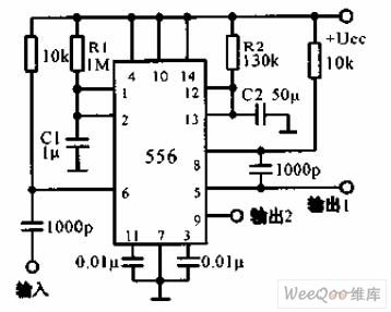
The diagram of sequential timer circuit composed of 556 is shown as above. 556 is a dual timer. The first timer output 1 passes 0.001μF coupling capacitor, then it isadded to the pin 8 of second timer's input end. The total delay is equal to two extension, 1 = 1.1 (R1C1 + R2C2). The wire connected to pin 6 is grounded, then the first timer can be turned on. (View)
View full Circuit Diagram | Comments | Reading(4951)
Timing control circuit diagram of vibrator
Published:2011/10/17 1:40:00 Author:Ecco | Keyword: Timing control , vibrator
View full Circuit Diagram | Comments | Reading(1701)
Automatic interval timer circuit composed of PUT
Published:2011/9/13 2:04:00 Author:Rebekka | Keyword: Automatic interval timer
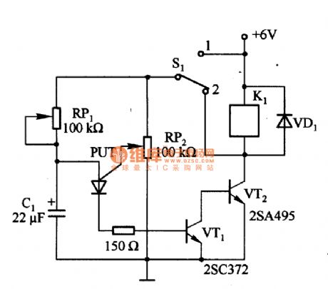
Figure 1 is composed of the PUT and other automatic interval timer circuit. In the circuit, PUT is the oscillator. Using the switch S1 to switchover the interval time and automatic time. When S1 connects to 1, it is automatic timing mode 1, thenS1connects to2, itis the interval time. If the resistance of RP2is too large, PUT anode current is less than the maintenance current, the circuit can not be used as the automatic timing circuit. (View)
View full Circuit Diagram | Comments | Reading(2327)
Cycle timing controller 5
Published:2011/8/9 20:15:00 Author:Ecco | Keyword: Cycle timing controller
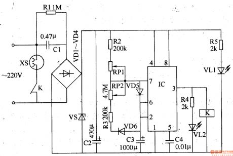
The cycle timing control circuit is composed of the power supply circuit and timing control circuit, and it is shown in Figure 3-93. The power supply circuit is composed of the step-down capacitor Cl, resistors Rl, R5, rectifier diodes VDl-VD4, voltage regulator diode VS, power indicator LED VLl and filter capacitor C2. Timing control circuit consists of the time-base IC, resistors R2-R4, capacitor C3, potentiometers RPl, RP2, diodes VD5, VD6, light-emitting diode VL2 and relay K. Rl selects the 1/2W carbon film resistor; R2-R5 use 1/4W carbon film resistors or metal film resistors. RP1 and RP2 select the small linear synthetic membrane potentiometers.
(View)
View full Circuit Diagram | Comments | Reading(1255)
| Pages:1/6 123456 |
Circuit Categories
power supply circuit
Amplifier Circuit
Basic Circuit
LED and Light Circuit
Sensor Circuit
Signal Processing
Electrical Equipment Circuit
Control Circuit
Remote Control Circuit
A/D-D/A Converter Circuit
Audio Circuit
Measuring and Test Circuit
Communication Circuit
Computer-Related Circuit
555 Circuit
Automotive Circuit
Repairing Circuit