
Time Control
Index 3
OVER_1_min
Published:2009/7/13 2:14:00 Author:May
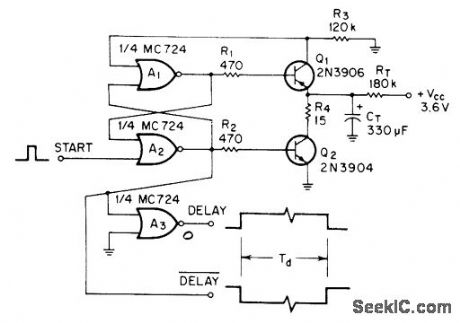
Circuit provides delays well over 1 min even with low operating voltages of ICs. When start pulse is applied to RS flip-flop A1-A2, Q2 turns off and allows RT to provide charging current for timing capacitor CT. When voltage across CT gets high enough, Q1 turns on and resets flip-flop, terminating delay period. A3 provides buffered complementary output.-R. W. Hilsher, Long-Delay Timer, EEEMagazine, Aug. 1970, p 79.
(View)
View full Circuit Diagram | Comments | Reading(860)
FET_TIMER_WITH_RELAY
Published:2009/7/13 2:12:00 Author:May
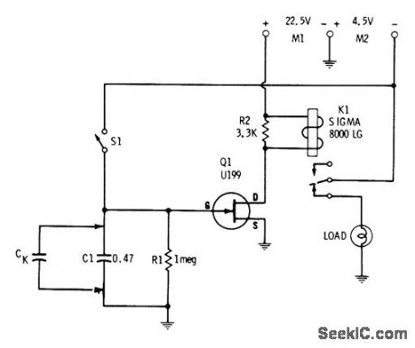
With values shown, circuit gives delay of several seconds. Increas-ing C1 bv shunting with 20-μF capacitor delays energizing of relay to over 1 min. C1 is charged to -4.5 V when switch S1 is closed, biasing gate to cutoff and deenergizing relay. When S1 is open, capacitor begins discharging at rate determined by RC time constant of circuit. When voltage across capacitordrops to point at which 01 conducts, relay is energized and power is applied to load.-E. M. Noll, FET Principles, Experiments, and Projects, Howard W. Sams, Indianapolis, IN, 2nd Ed., 1975, p 215-216. (View)
View full Circuit Diagram | Comments | Reading(1273)
FAlL_SAFE_LIGHT_TIMEB
Published:2009/7/13 1:49:00 Author:May
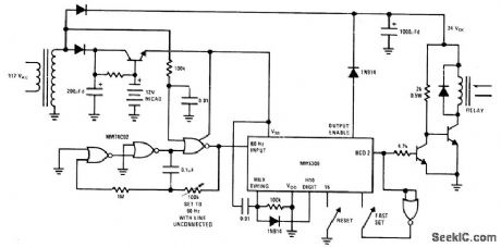
National MM5309 clock IC is used as timer in circuit that maintains timing with adequate accuracy during periods of power-line failure and retums automatically to 60-Hz line as soon as power is restored. Applications include control of lights in unoccupied home. Timing action tums on lights for 4h period every 24 h. When power is applied, intemal multiplex circuit strobes each digit until digit with connected diode is accessed. This digit stops multiplex scanning, and BCD outputs present data from selected digit as control waveform whose edges determine timer data.- MOS/LSI Databook, National Semiconductor, Santa Clara, CA, 1977, p 1.74-1-77. (View)
View full Circuit Diagram | Comments | Reading(913)
UJT_SCR_TIMER
Published:2009/7/13 1:47:00 Author:May
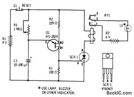
Use of large capacitance for C1 in simple UJT relaxation oscillator providestime delay action for triggering SCR controllingrelay R1 provides convenient adjustment ofdelay SCR can be 6-A 50-V Radio Shack 2761089. Relay is 275-004,-F.M.Mims, Semiconductor Projects, Vol 2, Radio Shack, Fort Worth,TX,1976,p 50-61. (View)
View full Circuit Diagram | Comments | Reading(2676)
10_s_TO_10_min
Published:2009/7/13 1:46:00 Author:May
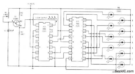
Away of ten LEDs serves for measuring time intervals up to 10 min, for timing phone calls, photographic exposures, and cooking. Pulse output rate of UJT oscillator Q1 is determined by value of C1 and setting of R1. Pulses are counted by 7490 which gives total count in binary form. 7490 recycles after each l0 counts. 7441 converts binary signals from 7490 to decimal outputs driving LED indicators. Each LED glows in sequence as count advances from 0 through 9 and repeats. For 10-pin timer, adiust R1 until first LED stays on for exactly 1 min. For 10-stimer, adiust R1 for blink rate of 1 s per LED.-F. M. Mints, Optoelectronic Proiects, Vol, n, Radio Shack, Fort Worth, TX, 1977, 2nd Ed., p 67-78. (View)
View full Circuit Diagram | Comments | Reading(870)
10_min_TIMER
Published:2009/7/13 1:35:00 Author:May
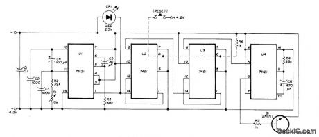
Uses SN74121 as actableMVBR generating pulses at 4-s intervals, U2 and U3 divide pulsetrain by 144 to give period of 576s U4 is then turned on, producing positive output pulse lasting 20 s that turns on Q1 for driving keyer, sidetone oscillator, lamp, or other signaling device as reminder for amateur radio operator to make 10-min station identification. R1 adjusts timing.-H. Seeger, Ten-Minute Timer, Ham Radio, Nov. 1976, p 66.
(View)
View full Circuit Diagram | Comments | Reading(1338)
Photo exposure timer circuit
Published:2011/8/4 3:24:00 Author:May | Keyword: Photo exposure timer
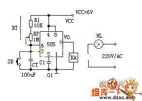
Working principle:
The photo exposure timer circuit is composed of 555 monostable circuit, which uses manually start monostable circuit. When the power is turned on, the timer will be in the steady state. At this point the voltage of the timing capacitor CT: VCT = VCC = 6V. The two inputs are in high level to this 555 equivalent trigger, that is, VS = 0. KA does not pull in, and the relay is opened, then the exposed lighting HL does not shine. This circuit provides parameters with about 1 second to 2 minutes delay time, which can be adjusted by potentiometer RP. The relay in the circuit must choose the products with the pull-in current being more than 30mA. (View)
View full Circuit Diagram | Comments | Reading(768)
1_YEAR_TIMER
Published:2009/7/12 22:41:00 Author:May
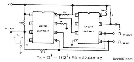
Cascaded operation of Exar XR-2242 long-range timers provides ultralong time delays, up to 1 year, Cascading of counter sections provides 32,640 clock cycles before output pin 3 of unit 2 changes state. Common pull-up resistor makes counter section of unit 2 trigger each time output of unit 1 makes positive-going transition. Cascading additional timer with unit 2 extends time delay to 1.065 x 10⁹RC. With RC values giving 0.1 s, time delay becomes 3.4 years.- Timer Data Book, Exar Integrated Systems, Sunnyvale, CA, 1978, p 19-22. (View)
View full Circuit Diagram | Comments | Reading(1033)
4_h_SEQUENTIAL_TIMER
Published:2009/7/12 22:32:00 Author:May
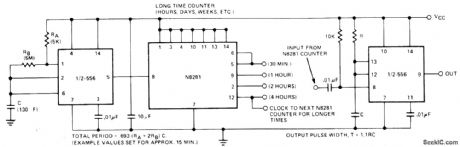
Use of N8281 divider network between sections of 556 dual time gives extremely long timedelays without costly large low-leakage capacitors. First section operates as oscillator having period of 1/f. Oscillator output is applied to divide-by-/N network to give output with period of N/f for triggering second half of timer. Connection of divider to second section determines amount of delay introduced by divider. Cascading of additional dividers increases maximum delay to days or even weeks.- Signetits Analog Data Manual, Signetics, Sunnyvale, CA, 1977, p 724. (View)
View full Circuit Diagram | Comments | Reading(1131)
LONG_TERM_ELECTRONIC_TIMER
Published:2009/7/7 3:57:00 Author:May
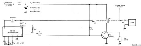
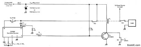
The timer includes an oscillator and a counter in an integrated circuit. The timing interval equals the oscillator period multiplied by the number of cycles to be counted.The oscillator frequency depends upon resistor RS and capacitor CX. The number of oscillator cycles to be counted before the counter output changes state is determined by the selection of the counter output terminal, shown here as pin 3. The interval can be set anywhere in the range from fractions of a second to months; it is given by T = 0.55 RSCX2n, where n is an integer determined by the counter-output selection.Operation is initiated by the closure of momentary switch S1 (or by a command signal having a similar effect). This grounds one side of relay K1, thereby activating the relay and causing the closure of the switches that supply power to the timer and to the load.The turn-on of VCC at the timer is coupled through C1 to the counter-reset terminal, thus resetting the counter. The initial reset voltage transient is then drained away through R1 to permit normal operation. During the first half cycle of the counter operation, the counter output voltage (at pin 3 in this case) is low. This tums on transistor Q1 so that relay K1 latches on, enabling the timer to continue running even though switch S1 has opened. The oscillator runs while the relay is on. When the number of oscillator cycles reaches the limit, the counter output voltage at pin 3 goes high. This tums off Q1, thereby tuming off the relay and returning the system to the original power-off state to await the next starting command. The timing cycle can also be interrupted and the system tumed off by opening normally-closed switch S2. (View)
View full Circuit Diagram | Comments | Reading(1034)
TWO_TONE_ALARM
Published:2009/7/6 21:07:00 Author:May
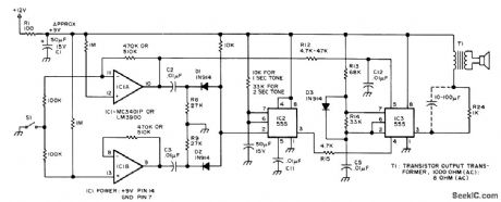
Provides audible backup for visual display in microprocessor-controlled system that requires human intervention under certain conditions, to alert operator who may be watching machinery rather than display. When input line goes high, device emits 1-s beep that means stop. When input goes low, 1-s lower-frequency boop sounds to indicate go. S1 represents signal derived from single-bit computer output. Audio bursts are generated by 555 timers, IC2 is wired as mono MVBR to determine tone duration, set by C4 and R11.Negative-going pulse on pin 2 triggers mono on. ff microprocessor circuit creates pulse rather than level change, input should go to pin 2. Tone frequency is set by C5, R13, and R14 of IC3. Trigger uses IC1A as inverting opamp and IC1B as noninverting opamp. Trigger outputs are differentiated to give negative-going spike for each input level change. Spikes are ORed by Dl and D2 for trigger input of IC2. Different tones are achieved by using IC1A to change input voltage to pin 5 of tone generator IC3. 0p-tional electrolytic capacitor across R24 will in-crease volume.-C. F. Douds, Audible Interrupts for Humans, BYTE, Feb. 1977, p 54 and 58. (View)
View full Circuit Diagram | Comments | Reading(944)
Electric Blanket And Rice Cooker Timer Circuit
Published:2011/7/28 6:55:00 Author:Robert | Keyword: Electric Blanket, Rice Cooker, Timer
The picture shows the electric blanket and rice cooker timer circuit. This circuit's timing time could be set from 1 second to more than 10 hours. In the picture, C1 is timing element. When the power supply is connected, pressing the switch AN1, the C1 would be charging to DC 28V. The comparator A would output high voltage level and the transistor VT would be connected, the relay J would be powered up and have actions. The J1-1 would be conncted and the power would be self-locked. The J1-2 would be disconnected. C1 would discharge to the high-resistance input port. When the C1's voltage is decreased and lower than the A's out-phase input port, the A would output low voltage level, the transistor VT would be disconnected, J would lost the power and be released. Then the timing is over until next case that the timing trigger switch AN1 is pressed again. (View)
View full Circuit Diagram | Comments | Reading(3115)
UP_TO_1OO_kHz_WITH_322_TIMER
Published:2009/7/2 1:07:00 Author:May
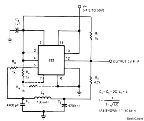
Efficient LC oscillator uses IC timer as inverting comparator, with pinetwork LC tank as resonant circuit. Output square wave is regulated to 3 V in amplitude, independently of supply voltage; upper supply limit should be 40 V instead of value shown. Sine-wave output of oscillator may also be used extemally by adding single-supply opamp as buffer. Values shown give 10 kHz, but upper limit is 100 kHz.-W. G. Jung, Take a Fresh Look at New IC Timer Applications, EDN Magazine, March 20, 1977, p 127-135. (View)
View full Circuit Diagram | Comments | Reading(1832)
ENLARGER_TIMER
Published:2009/7/1 21:24:00 Author:May
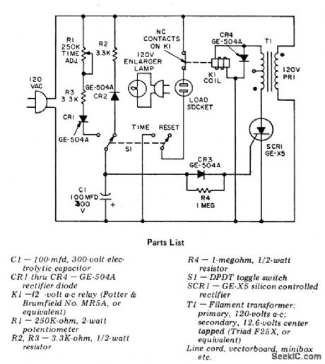


Circuit NotesThis precision, solid state, time delay circuit has delayed off and delayed on switch-ing functions that are interchangeably available by simply interchanging the relay contacts. (View)
View full Circuit Diagram | Comments | Reading(0)
DC_VOLTAGE_TO_TIME
Published:2009/6/30 21:02:00 Author:May
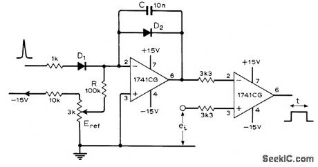
Opamp connected as integrator feeds opamp comparator to produce output pulse whose width is proportional to magnitude of DC input voltage. Circuit shown is for positive inputs only; for both positive and negative inputs, article tells how to add another comparator. Circuit can then be used to generate start and stop pulses applied to digital timer of digital voltmeter.—G. B. Clayton, Experiments with Operational Amplifiers, Wireless World, Sept. 1973, p 447-448. (View)
View full Circuit Diagram | Comments | Reading(944)
Fast reverse amplifier with high input impedance circuit
Published:2011/7/28 4:17:00 Author:John | Keyword: Fast reverse amplifier, high input impedance
Fast reverse amplifier with high input impedance circuit is shown.
(View)
View full Circuit Diagram | Comments | Reading(729)
SIMPLE_TIME_DELAY
Published:2009/6/29 2:40:00 Author:May
View full Circuit Diagram | Comments | Reading(0)
TIMER
Published:2009/6/29 2:39:00 Author:May
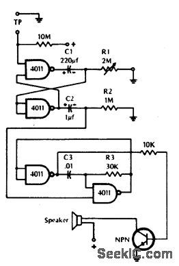
The timer can be used wherever time periods of up to seven minutes duration are needed. To turn on just touch the turn-on plate, and after the selected time has elapsed, an alarm will sound for a short period, then au-tomatically turn off. The turn-on touch plate, labeled TP in the diagram, is made up of two metal strips about 1/16-inch apart. Bridging the gap with your finger activates the timer. For more time range, increase RI and/or C1. R2 and C2 determine the period of time that the alarm will sound. Increasing either will extend the time. The tone of the alarm is determined by R3 and C3. Increasing either lowers the tone, decrqasing them raises the tone. (View)
View full Circuit Diagram | Comments | Reading(1097)
741_TIMER
Published:2009/6/29 2:37:00 Author:May
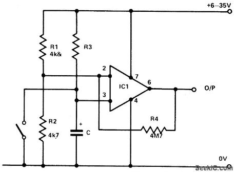
R1 and R2 hold the inverting input at half supply voltage. R4 applies feedback to increase the input impedance at pin 3. Pin 3, the nonin-verting input, is connected to the junction of R3 and C. Afterthe switch is opened, C charges via R3. When the capacitor has charged sufficiently for the potential at pin 3 to exceed that at pin 2 the output abruptly changes from 0 V to positive line potential. If reverse polarity operation is required, simply transpose R3 and C. R3 and C can be any values. Time delays from a frac-tion of a second to several hours can be ob-tained by judicious selection. The time delay-independent of supply voltage-is 0.7CR seconds where C is in farads. (View)
View full Circuit Diagram | Comments | Reading(1874)
LONG_INTERVAL_RC_TIMER
Published:2009/6/29 2:35:00 Author:May
View full Circuit Diagram | Comments | Reading(733)
| Pages:3/6 123456 |
Circuit Categories
power supply circuit
Amplifier Circuit
Basic Circuit
LED and Light Circuit
Sensor Circuit
Signal Processing
Electrical Equipment Circuit
Control Circuit
Remote Control Circuit
A/D-D/A Converter Circuit
Audio Circuit
Measuring and Test Circuit
Communication Circuit
Computer-Related Circuit
555 Circuit
Automotive Circuit
Repairing Circuit