
Electrical Equipment Circuit
Index 110
The principle circuit diagram of electric bicycle
Published:2011/5/11 1:54:00 Author:Rebekka | Keyword: electric bicycle
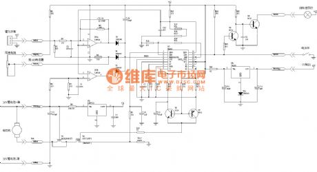
Here is the diagram of electric bicycle principle circuit. (View)
View full Circuit Diagram | Comments | Reading(3055)
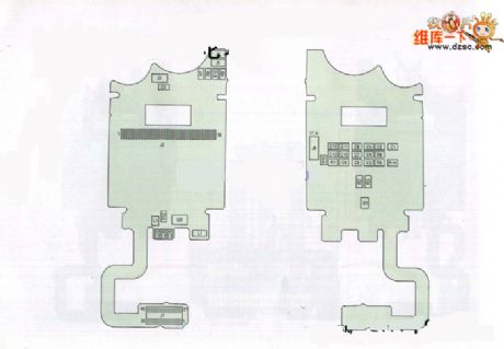
ZTE C700 mobile phone wire arrangement component distribution map
Published:2011/5/11 3:19:00 Author:Nicole | Keyword: ZTE, mobile phone, wire arrangement component
View full Circuit Diagram | Comments | Reading(676)
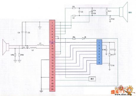
ZTE 767+ type mobile phone wire arrangement circuit schematic diagram
Published:2011/5/11 3:15:00 Author:Nicole | Keyword: ZTE 767+ type, mobile phone, wire arrangement
View full Circuit Diagram | Comments | Reading(1251)
CD2003—AM/FM radio monolithic integrated circuit
Published:2011/5/10 1:14:00 Author:Fiona | Keyword: radio monolithic integrated
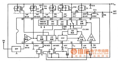
CD2003 is an AM / FM radio monolithic integrated circuit,it has been widely used in the desheng series radio.1. Features
CD2003 integrated circuit contains AM HF amplifier, local oscillator, mixer, IF amplifier and detector circuit ;FM HF amplifier, local oscillator, mixer, IF amplifier and discriminator circuit : and the AGC circuit, AM / FM band selection circuit etc, the block diagram of the in-circuit is shown in Figure 1.
Figure 1 CD2003 integrated circuit within the circuit block diagram and typical application circuit2.pin functions and data
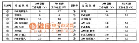
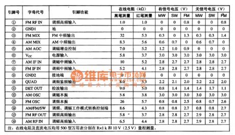
CD2003 integrated circuit uses 16-pin dual in-line Package,the pin functions and typical operating parameters(Vcc = 3V time, the pin voltage in AM and FM both cases,) are listed in table 1,the pin function and the test data on the desheng multi-band radio are listed in the table 2.
Table 1 CD2003 integrated circuit pin functions and typical operating parameters
Table 2 CD2003 integrated circuit pin functions and test data on the desheng multi-band radio
3.Typical application circuit
Illustration 1 is a typical application circuit of AM / FM band radio formed by the CD2003 integrated circuit.the work process1) AM band.The signals received from Antenna input from the CD2003 (16) pin ,mixing with the LO signal in the mixing circuit.The signal obtained output from (4) pin , obtaining the 465kHz IF signal selected by frequency to input from the (7) pin.After being converted by the IF amplification, detection, electronic switch, the signals output from (11) pin to reach the post-stage circuit. (2)FM band.The signals received from Antenna input from the (1) pin after being band-pass filtered by the BPF,added to the mixing circuit after HF amplifier.Mixing with the LO signal in the mixing circuit,the signal obtained output from (3) pin , obtaining the 10.7MHz IF signal selected by frequency to input from the (8) pin.After being converted by the AM / FM electronic switch, the signals output from (11) pin to reach the post-stage circuit.Tip:According to the above-mentioned signal flow ,it's convenient to repair AM or FM radio with sound or radio trouble.Becauce CD2003 will not easily damaged,we should pay attention to the periphery of its three-terminal filters to be checked. (View)
View full Circuit Diagram | Comments | Reading(24578)
Environmental Temperature Effects On The Non-Operating Current And Operating Current Circuit
Published:2011/5/11 1:25:00 Author:Robert | Keyword: Environmental Temperature, Non-Operating Current, Operating Current
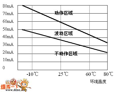
The Environmental Temperature Effects On The Non-Operating Current And Operating Current Circuit is shown below.
1.The maximum working voltage.PTC thermistor is in series in the circuit. When normally working it only has little voltage kept on the PTC thermistor. If the PTC thermistor starts in high impedance status, it would stand nearly the whole power supply voltage. So it should have large enough standing voltage while choosing PTC thermistor, and also should consider the possible wave motion caused by the power supply voltage.2.Non-operating current and operating current.To achieve stable switch functions, the operating current should be at least double of the non-operating current.Because of the environmental temperature's effects on the non-operating current and operating current is so big (see picture 1), the worst case should take into account. For non-operating current, it's best to choose the value at the available maximum environmental temperature. For operating current, it's best to choose the value at the available low environmental temperature.3.Available maximum current at the maximum working voltage.If requiring the PTC thermistor to run the protection function, it needs to check out if the circuit has the conditions of producing larger than the available maximum current, which generally means the possible short circuit situation of the users' application. The specifications document has given the maximum current value, and when using exceeding this value it may cause the PTC thermistor broken or early disabled.
(View)
View full Circuit Diagram | Comments | Reading(601)
Sitting Posture Reminder Device Circuit (2)
Published:2011/5/11 1:27:00 Author:Robert | Keyword: Sitting Posture, Reminder
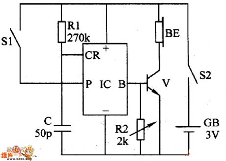
The sitting posture reminder device introduced in this example, should be hung on the user's ears or be installed on the hats when using. When the user's upper body or head has a big front-lean angle it would give out the voice reminder tone: Please note the myopia!Sit upright quickly! or Please note the sitting posture! . This device can not only be used for the office staffs and students' sitting posture correction, myopia protection, but also can be used as the sleep reminder for the motor vehicle drivers.The circuit's working principle is shown below.This sitting posture reminder is made up by the mercury switch (as front-lean angle sensor) S1, resistance R1, R2, capacitor C, voice integrated circuit IC, transistor V, earphone BE, power switch S2 and battery GB which is shown in the picture below.In normal time (the user's sitting posture is correct), the mercury switch S1 is disconnected, IC do not work, BE has not sound. When the user's head has a certain front-lean angle the S1 is connected to trigger IC to work. It outputs the voice electrical signal which is amplified by V and then this signal drives BL to play the voice reminder tone.The angle which trigger the alarm sound can be changed by adjusting S1's position.The tone played by BE can be adjusted by changing R2's value.
(View)
View full Circuit Diagram | Comments | Reading(855)
Sitting Posture Reminder Device Circuit (1)
Published:2011/5/11 1:29:00 Author:Robert | Keyword: Sitting Posture, Reminder

When the primary and secondary students are reading or writing, if their sitting posture is not correct for a long time, it would easily affect their vision and physical health. The sitting posture reminder device introduced in this example can remind the users when their reading or writing posture is not correct by giving out the sound: DD or voice reminder tone. So it can remind the user to note their posture and fix it.The circuit's working principle is shown below.This sitting posture reminder device circuit is made up by electronic switch circuit GB, alarm circuit and power circuit which is shown in the picture below.The electronic switch circuit is made up by glass shell mercury switch S2, transistor V1, V2 and resistance R1~R3.The power circuit is made up by power GB and power switch S1.When he power switch S1 is connected, the power GB would be supply the whole circuit with the working voltage.When the user's reading or writing posture is correct, the mercury switch S2 would be disconnected and the transistor V1 and V2 are all disconnected. The integrated circuit IC is not working and BL has no sound.When the user's sitting posture is front-lean (near the desktop), the S2 would be connected and V1 and V2 are al connected. V2's emitter output high voltage level to the IC's TRIG port to trigger the IC to work. Then its output port (OUT) would output the audio signal, which is amplified by V3, to drive the speaker to give out the DD' alarm sound or play the voice reminder tone: Please note myopia! Sit upright quickly! .
(View)
View full Circuit Diagram | Comments | Reading(810)
W723 High-Voltage Current-Limiting Protection Circuit
Published:2011/5/7 6:03:00 Author:Robert | Keyword: High-Voltage, Current-Limiting, Protection


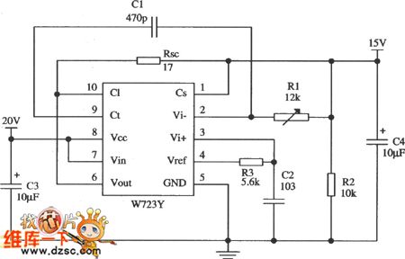
The application circuit shown in the picture below with output voltage higher thanreferenced voltage is composed of the W723 multi-port adjustable positive stabilizer. There is current limiting protectionin this circuit and the output voltage is adjustable from 7V to 36V. The input voltage in the picture is 20V, and its output voltage is 15V. The circuit in the picture also changes the output voltage by changing the sample resistance's voltage partial pressure ratio. The R2's caculation method is shown below. In its formula Vref is the referenced voltage of the stabilizer which is about 7.2V; the current-limiting resistance R3's caculation is shown below which can be taken 17Ω.
(View)
View full Circuit Diagram | Comments | Reading(1510)
Current Limiting Protection Application Cirrcuit Composed of WB705
Published:2011/5/8 6:43:00 Author:Robert | Keyword: Current Limiting, Protection, Application
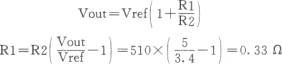

The picture shown below is about the current-limiting protection application cirrcuit with output voltage of 5V and output current of 1.5A which is composed of WB718 multi-port adjustable positive integrated stabilizer. The input voltage of the circuit can be maximum 16.8V and minimum 12.1V. The C1 and C2 are filter capacitors whose value can be choosed based on the current value. The more load current is, the more the capacitor value is required, which would reduce the ripple value of the stabilizer input port. C3 is a compensation capacitor used to prevent the oscillation effects. If the circuit has no oscillation, C3's value can be considerable less. Because C3 is connected directly to the stabilizer internal amplifier through its 7 foot. If its value is too big, that will influence the magnification. C4 can make the variation value of output voltage ΔVout to couple directly to the 6 foot of the stabilizer internal sampling port which can improve ripple rejection ratio. C5 and C6 is the capacitor to output filter wave. R1 and R2 is sampling resistance and they suit for the formula shown below. In its formula, Vref is the stabilizer's base referenced voltage with value of 3.4V. Because Vref has some extent discrete features, it should be a little bigger than the caculation result of R1 when it's chosen to use.
(View)
View full Circuit Diagram | Comments | Reading(652)
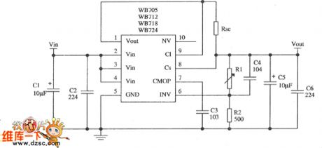
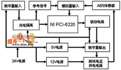
ABS Program Test Flow Circuit
Published:2011/5/10 7:40:00 Author:Robert | Keyword: ABS, Program Test Flow
The ABS Program Test Flow Circuit is shown below.
(View)
View full Circuit Diagram | Comments | Reading(638)
TII Interface Circuit
Published:2011/5/9 19:18:00 Author:Robert | Keyword: TII, Interface
The TII Interface Circuit is shown below.
(View)
View full Circuit Diagram | Comments | Reading(585)
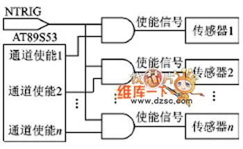
ABS Sensor Interface Board Structure Circuit
Published:2011/5/10 7:43:00 Author:Robert | Keyword: ABS, Sensor Interface Board, Structure
The ABS Sensor Interface Board Structure Circuit is shown below.
(View)
View full Circuit Diagram | Comments | Reading(666)
PR4101 Typical Application Circuit
Published:2011/5/10 7:54:00 Author:Robert | Keyword: Typical Application
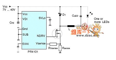
The PR4101 Typical Application Circuit is shown below.
(View)
View full Circuit Diagram | Comments | Reading(657)
PR4101 Pane Circuit
Published:2011/5/10 7:53:00 Author:Robert | Keyword: Pane
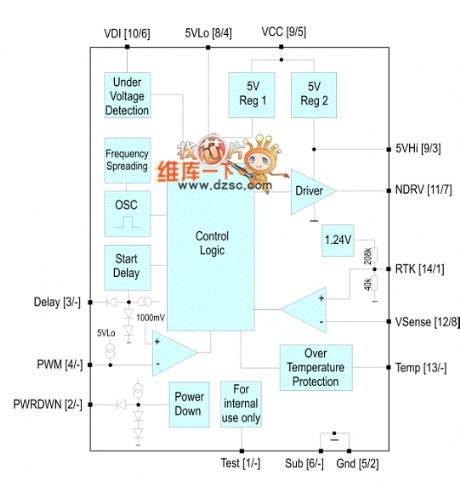
The PR4101 Pane Circuit is shown below.
(View)
View full Circuit Diagram | Comments | Reading(559)
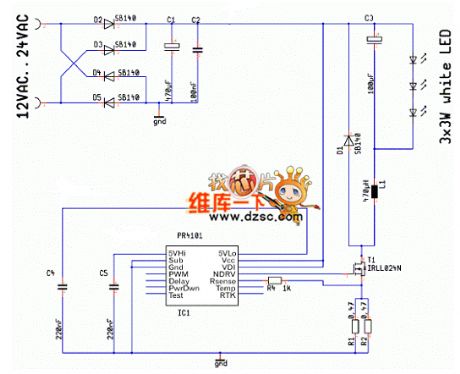
PR4101 Application Circuit Using 12/24V Power
Published:2011/5/10 7:52:00 Author:Robert | Keyword: Application, 12/24V Power
The PR4101 Application Circuit Using 12/24V Power is shown below.
(View)
View full Circuit Diagram | Comments | Reading(606)
PR4101 Application Circuit Using 12VDC
Published:2011/5/10 7:50:00 Author:Robert | Keyword: Application, 12VDC

The PR4101 Application Circuit Using 12VDC is shown below.
(View)
View full Circuit Diagram | Comments | Reading(592)
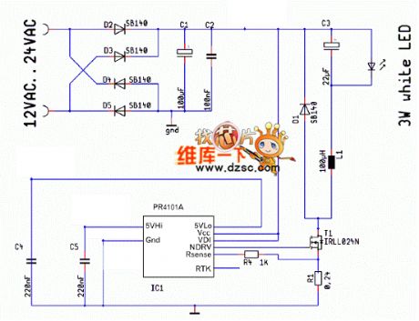
PR4101 Application Circuit Using 12VAC
Published:2011/5/10 7:49:00 Author:Robert | Keyword: Application, 12VAC
The PR4101 Application Circuit Using 12VAC is shown below.
(View)
View full Circuit Diagram | Comments | Reading(574)
PR4101 Display Plate Circuit
Published:2011/5/10 5:14:00 Author:Robert | Keyword: Display Plate
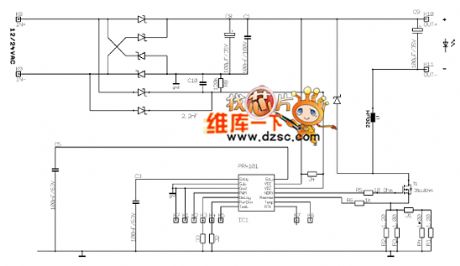
The PR4101 Display Plate Circuit is shown below.
(View)
View full Circuit Diagram | Comments | Reading(604)
The Close-Function Circuit Of LM94022 Connecting With Two-Input AND Gate
Published:2011/5/9 8:50:00 Author:Robert | Keyword: Close-Function, Two-Input AND Gate
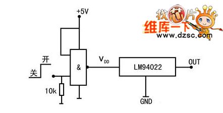
The close-function circuitof LM94022 connecting with two-input AND gateis shown below.
(View)
View full Circuit Diagram | Comments | Reading(560)
HRBCD-230A-An Single Door PC Intergrated Circuit of Refrigerator
Published:2011/5/10 10:33:00 Author:Borg | Keyword: Intergrated Circuit, Single Door
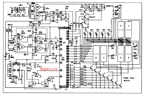
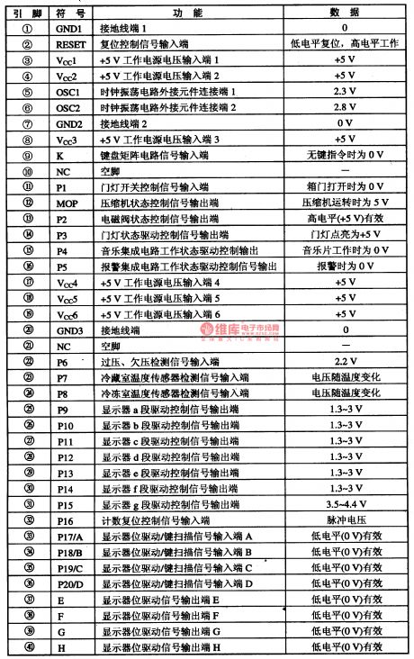
HRBCD-230A is a single door PC intergrated circuit developped by Huari Company, which is specially used in refrigerators.
1.typical application circuit
Besides fullfilling the common control functions, the HRBCD-230A can also monitor the grid voltage, memorize the starting/turning off time of the compressor, start the power delay relay of the compressor and monitor the overvoltage and undervoltage, therefore protects the compressor when it works too long. The typical application circuit of the chips is listed in Table 1-1.
Figure 1-1 the typical application circuit of the chips
Table 1-1 the HT664L pin functions of the decoding intergrated circuit (View)
View full Circuit Diagram | Comments | Reading(746)
| Pages:110/126 At 20101102103104105106107108109110111112113114115116117118119120Under 20 |
Circuit Categories
power supply circuit
Amplifier Circuit
Basic Circuit
LED and Light Circuit
Sensor Circuit
Signal Processing
Electrical Equipment Circuit
Control Circuit
Remote Control Circuit
A/D-D/A Converter Circuit
Audio Circuit
Measuring and Test Circuit
Communication Circuit
Computer-Related Circuit
555 Circuit
Automotive Circuit
Repairing Circuit