
Index 140
3_A_positive_adjustable_voltage_regulator
Published:2009/7/23 23:22:00 Author:Jessie
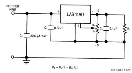
The LAS14AU is a four-terminal adjustable regulator IC with an output range from +4 to +30V, providing remote-sense capability with a single pot. Characteristics are shown in Fig. 7-28B, 7-28C, and 7-28D. (View)
View full Circuit Diagram | Comments | Reading(823)
High_stability_linear_regulator
Published:2009/7/23 23:19:00 Author:Jessie

The load and line regulation of this circuit is better than 0.001%.Noise, drift, and long-term stability are determined by Zener D1. Noise can be reduced by inserting 100-kΩ resistors in series with both inputs of the LM108A, and bypassing the noninverting input to ground. A 100-pF capacitor between the LM108A output and the inverting input prevents frequency stability. Temperature drift can be reduced by adjusting R4 for minimum drift. For best results, remote sensing should be made directly to the load terminals, as shown. (View)
View full Circuit Diagram | Comments | Reading(813)
Very_wide_range_V_F_converter
Published:2009/7/23 23:18:00 Author:Jessie
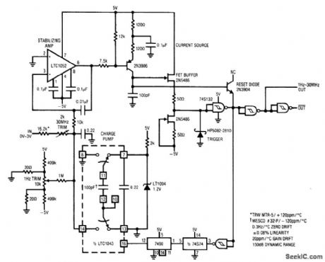
Fig. 12-4 This circuit is a highly modified version of the circuit in Fig. 12-3 and it features a range from 1 Hz to 30 MHz. The circuit maintains a 0.08% linearity over the entire range with a full-scale drift of about 20 ppm/℃. Zero-point error is 0.3 Hz/℃ (and is directly related to the 50 nV/℃ drift specification of the LTC1052). To trim, ground the input and adjust the 1-Hz trim until oscillation just starts. Next, apply 3.000 V and set the 30-MHz trim for a 30.00-MHz output. Repeat the procedure until both points are fixed. Linear Technology Linear Applications Handbook 1990, p AN9-15. (View)
View full Circuit Diagram | Comments | Reading(614)
Improved_linear_current_regulator
Published:2009/7/23 23:18:00 Author:Jessie
This circuit is similar to that of Fig. 7-13, except that the addition of C1 prevents oscillation. (View)
View full Circuit Diagram | Comments | Reading(602)
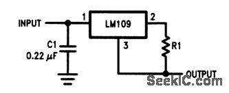
Simple_5_V_adjustable_regulator
Published:2009/7/23 23:17:00 Author:Jessie
This circuit is similar to that of Fig. 7-24, except that the output is adjustable (above 5 V). (View)
View full Circuit Diagram | Comments | Reading(552)
3_A_positive_fixed_voltage_regulator
Published:2009/7/23 23:21:00 Author:Jessie
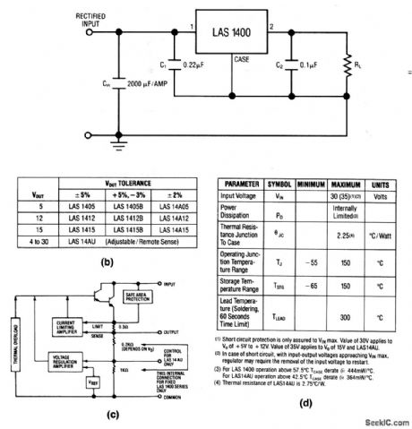
The LAS1400 series voltage regulators are ICs that contain all elements necessary for linear regulation (safe-area protection, thermal overload, current limiting, as shown in Fig. 7-28C). Figure 7-28B shows the output voltage and tolerance for the various LAS1400 part numbers. Figure 7-28D shows the absolute maximum ratings. (View)
View full Circuit Diagram | Comments | Reading(654)
Fast_V_F_converter
Published:2009/7/23 23:20:00 Author:Jessie
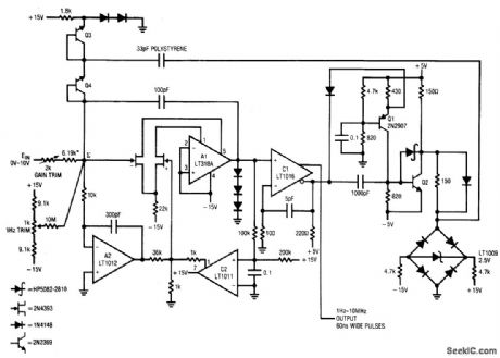
Fig. 12-5 This circuit features a range from 1 Hz to 10 MHz with a linearity of 0.06%, and a typical full-scale drift of 50 ppm/℃. The zero-point error is about 0.2 μV/℃ (or 0.2 Hz/℃). To trim, ground the input and adjust the 1-Hz trim for 1-Hz output. Next, apply 10.000 V and adjust the gain trim for 10.000-MHz output. Repeat the procedure until both points are fixed. Linear Technology, Linear Applications Handbook, 1990 p AN13-9. (View)
View full Circuit Diagram | Comments | Reading(664)
3_A_positive_adjustable_current_regulator
Published:2009/7/23 23:25:00 Author:Jessie
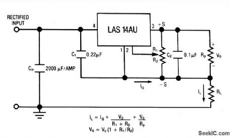
This circuit uses the LAS14AU voltage-regulator IC (Fig. 7-29) as an adjustable-current regulator. Characteristics are shown in Fig. 7-28B, 7-28C, and 7-28D. (View)
View full Circuit Diagram | Comments | Reading(691)
High_speed_15_A_MOSFET_drivers
Published:2009/7/23 23:24:00 Author:Jessie
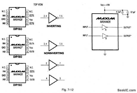
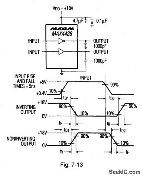
Figure 7-12 shows the basic connections for the MAX4426/27/28 drivers. Such ICs rapidly charge and discharge the gate capacitance of the largest MOSFETs to within millivolts of the supply. The typical on resistance is 4 Ω, the delay times are 10 ns for tD1 and 25 ns for tD2, the peak output current is 1.5 A, rise and fall times are typically 20 ns with 1000-pF loads, the operating range is 4.5 V to 18 V, and the power consumption is 1.8 mA with a logic-1 output and 200 μA with a logic-0 input. The ICs are TTL/CMOS compatible and will withstand greater than 500-mA reverse current. Figure 7-13 is a test circuit. Maxrvt HIGH-RELIABILITY DATA BOOK, 1993, P. 4-5, 4-6.
(View)
View full Circuit Diagram | Comments | Reading(804)
Simple_fast_V_F_converter
Published:2009/7/23 23:29:00 Author:Jessie
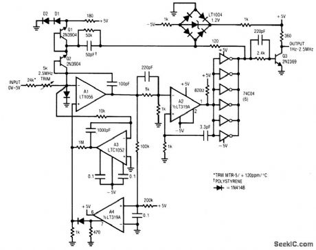
Fig. 12-8 The 2.5-MHz output of this circuit settles from a full-scale input in 3μs while maintaining 0.05% linearity with 50 ppm/℃ drift. To trim, apply 5.000 V and adjust the 2.5MHz trim for 2.500 MHz at the output. No zero trim is required. A TTL-compatible (5 V) output is available at the Q3 collector. Linear Technology. Linear Applications Handbook 1990, p AN14-4. (View)
View full Circuit Diagram | Comments | Reading(799)
15_A_positive_adjustable_voltage_regulator
Published:2009/7/23 23:29:00 Author:Jessie
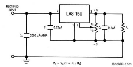
The LAS15U is a four-terminal adjustable regulator IC with an output range from +4 to +30 V, providing remote-sense capability with a single pot. Characteristics are shown in Fig.7-32B, 7-32C, and 7-32D. (View)
View full Circuit Diagram | Comments | Reading(821)
15_A_positive_fixed_voltage_regulator
Published:2009/7/23 23:28:00 Author:Jessie
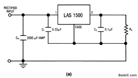
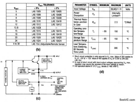
The LAS1500 series voltage regulators are ICs that contain all elements necessary for linear regulation (safe-area protection, thermal overload, and current limiting, as shown in Fig. 7-32C). Figure 7-32B shows the output voltage and tolerance for the various LAS1500 part numbers. Figure 7-32D shows the absolute maxirnum ratings. (View)
View full Circuit Diagram | Comments | Reading(667)
8_A_positive_fixed_voltage_regulator
Published:2009/7/23 23:52:00 Author:Jessie
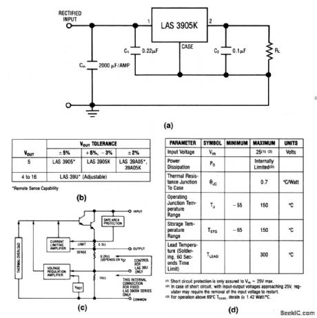
The LAS3905 series voltage regulators are ICs that contain all elements necessary for linear regulation (safe-area protection, thermal overload, and current limiting, as shown in Fig. 7-50C). Figure 7-50B shows the output voltage and tolerance for the various LAS3905 part numbers. Figure 7-50D shows the absolute maximum ratings. (View)
View full Circuit Diagram | Comments | Reading(800)
14_VOLT,4_AMP_BATTERY_CHARGER_POWER_SUPPLY
Published:2009/7/3 4:18:00 Author:May
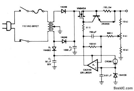
Operation amplifier A1 directly drives the VN64GA with the error signal to control the output voltage. Peak rectifier D1, C1 supplies error amplifier A1 and the reference zener. This extra drive voltage must exceed its source voltage by several volts for the VN64GA to pass full load current. The output voltage is pulsating dc which is quite satisfactory for battery charging. To convert the system to a regulated dc supply, capacitor C2 is increased and another electrolytic capacitor is added across the load. The response time is very fast, being determined by the op-amp. The 2N4400 current limiter circuit prevents the output current from exceeding 4.5 A. However, maintaining a shorted condition for more than a second will cause the VN64GA to exceed its temperature ratings.A generous heat sink, on the order of 1℃/W, must be used. (View)
View full Circuit Diagram | Comments | Reading(1605)
VERSATILE_BATTERY_CHARGER
Published:2009/7/3 4:15:00 Author:May
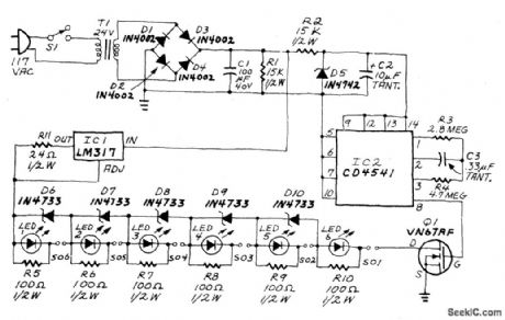
An LM317 voltage regulator is configured as a constant-current source. It is used to supply the 50 mA charging current to S01-S06, an array of AA-cell battery holders. Each of the battery holders is wired in series with an LED and its associated shunt resistor. When the battery holder contains a battery, the LED glows during charging. Each battery holder/LED combination is paralleled by a 5.1-volt Zener diode. If the battery holder is empty, the Zener conducts the current around the holder.A timing circuit prevents overcharging. When power is applied to the circuit, timing is initiated by IC2, a CD4541 oscillator/programmable timer. The output of IC2 is fed to Q1. When that output is high, the transistor is on, and the charging circuit is completed.When the output is low, the transistor is off, and the path to ground is interrupted. (View)
View full Circuit Diagram | Comments | Reading(2685)
Timer_F_V_converter
Published:2009/7/23 23:52:00 Author:Jessie

Fig.12-18 This circuit uses an LM122 timer as a basic F/V converter. The LM122 timer as a basic F/V converter. The LM122 output pulses are averaged with a simple one-pole filter to provide a dc output that is directly related to the trigger input frequency. The pulse width is adjusted with R2 to provide initial calibration at 10kHz. Linearity is about 0.2% for a 0-to 1-V output. A series RC network across the meter provides damping and will improve response at very low frequencies. (View)
View full Circuit Diagram | Comments | Reading(1483)
Negative_step_up_dc_dc_converter
Published:2009/7/23 23:51:00 Author:Jessie
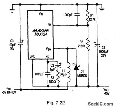
Figure 7-22 shows the MAX724 connected to provide a -15-V output with a -5-V to -15-V input. See Figs. 7-18 and 7-19 for pin configurations, and Fig. 7-20 for component suppliers. MAXIM EVALUATION KIT DATA Book, 1994, P. 3-138. (View)
View full Circuit Diagram | Comments | Reading(822)
5_A_positive_adjustable_current_regulator
Published:2009/7/23 23:51:00 Author:Jessie
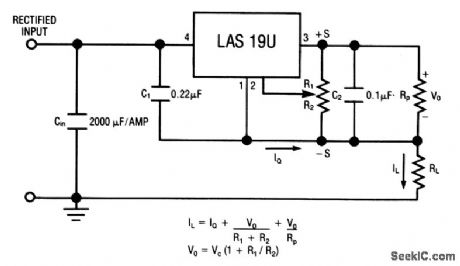
This circuit uses the LAS19U voltage-regulator IC (Fig. 7-47) as an adjustable-current regulator. Characteristics are shown in Fig. 7-46B, 7-46C and 7-46D. (View)
View full Circuit Diagram | Comments | Reading(1007)
BATTERY_CHARGER_OPERATES_ON_SINGLE_SOLAR_CELL
Published:2009/7/3 4:11:00 Author:May
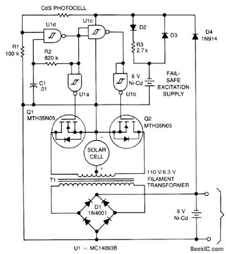
The circuit charges a 9-V battery at about 30 mA per input ampere at 0.4 V. U1, a quad Schmitt trigger, operate as an astable multivibrator to drive push-pull TMOS devices Q1 and Q2. Power for U1 is derived from the 9-V battery via D4; power for Q1 and Q2 is supplied by the solar cell. The multivibrator frequency, determined by R2-C1, is set to 180 Hz for maximum efficiency from a 6.3-V filament transformer, T1. The secondary of the transformer is applied to a full wave bridge rectifier, D1, which is connected to the batteries being charged. The small Ni-Cad battery is a fail-safe excitation supply to allow the system to recover if the 9-V battery becomes fully discharged.A CdS photocell shuts off the oscillator in darkness to preserve the fail-safe battery during shipping and storage, or prolonged darkness (View)
View full Circuit Diagram | Comments | Reading(1151)
2_A_positive_fixed_voltage_regulator
Published:2009/7/23 23:34:00 Author:Jessie
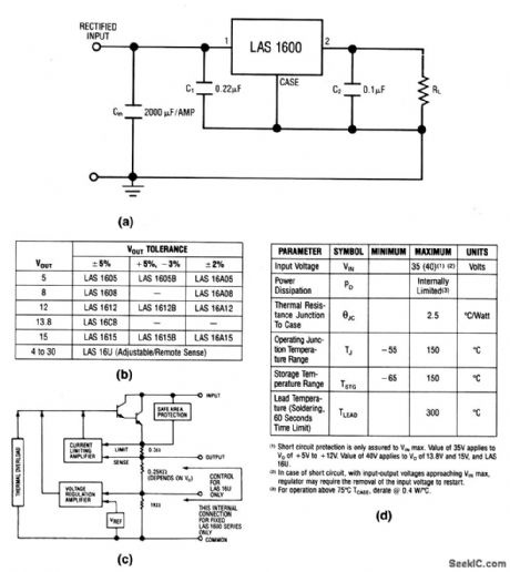
The LAS1600 series voltage regulators are ICs containing all elements necessary for linear regulation (safe-area protection, thermal overload, current limiting, as shown in Figure 7-37C). Figure 7-32B shows the output voltage and tolerance for the various LAS1600 part numbers. Figure 7-37D shows the absolute maximum ratings. (View)
View full Circuit Diagram | Comments | Reading(719)
| Pages:140/291 At 20121122123124125126127128129130131132133134135136137138139140Under 20 |
Circuit Categories
power supply circuit
Amplifier Circuit
Basic Circuit
LED and Light Circuit
Sensor Circuit
Signal Processing
Electrical Equipment Circuit
Control Circuit
Remote Control Circuit
A/D-D/A Converter Circuit
Audio Circuit
Measuring and Test Circuit
Communication Circuit
Computer-Related Circuit
555 Circuit
Automotive Circuit
Repairing Circuit