
Index 141
Step_up_PWM_regulators
Published:2009/7/23 23:33:00 Author:Jessie
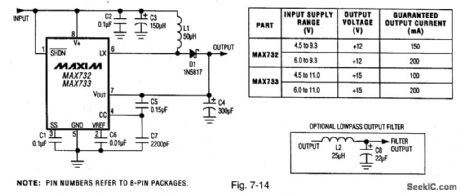
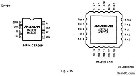
Figure 7-14 shows the MAX732 and MAX733 connected as step-up PWM (pulse-width modulation) regulators. Typical efficiency for the MAX731 is 82% to 87%, with 85% to 95% for the MAX733. Figure 7-15 shows the pin configurations. MAXIM HIGH-RELIAsILITY DATA BOOK, 1993, P. 4-65. (View)
View full Circuit Diagram | Comments | Reading(703)
WIND_POWERED_BATTERY_CHARGER
Published:2009/7/3 4:06:00 Author:May

The dc motor is used as a generator with the voltage output being proportional to its rpm. The LTC1042 monitors the voltage output and provides the following control functions.
1. If generator voltage output is below 13.8 V, the control circuit is active and the Ni-Cad battery is charging through the LM334 current source. The lead acid battery is not being chirged.2. If the generator voltage output is between 13.8 V and 15.1 V, the 12 V lead acid battery is being charged at about 1 amp/hour rate (limited by the power FET).3. If generator voltage exceeds 15.1 V (a condition caused by excessive wind speed or 12 V battery being fully charged) then a fixed load is connected limiting the generatorrpm to prevent damage.
This charger can be used as a remote source of power where wind energy is plentiful such as on sailboats or remote radio repeater sites. Unlike solar powered panels, this system will function in bad weather and at night. (View)
View full Circuit Diagram | Comments | Reading(4057)
BATTERY_CHARGER
Published:2009/7/3 4:03:00 Author:May
The charger is based on a charging voltage of 2.4 V per cell, in accordance with most manufacturers' recommendations. The circuit pulses the battery under charge with 14.4 V (6 cells × 2.4 V per cell) at a rate of 120 Hz. The design provides current limiting to protect the charger's internal components while limiting the charging rate to prevent damaging severely discharged lead-acid batteries. The maximum recommended charging current is normally about one-fourth the ampere-hour rating of the battery. For example, the maximum charging current for art average 44 ampere-hour battery is11 A. If the impedance of the load requires a charging current greater than the 11 A current limit, the circuit will go into current limiting. The amplitude of the charging pulses is controlled to maintain a maximum peak charging current of 11 A (8 A average). (View)
View full Circuit Diagram | Comments | Reading(4096)
Single_cell_V_F_converter__25_Hz_to_10_kHz
Published:2009/7/23 23:51:00 Author:Jessie
Fig. 12-1 7 This circuit is similar to that of Fig. 12-11, except that a 0- to 1-V input produces a 25-Hz to 10-kHz output. Transfer linearity is 0.25%, drift is 250 ppm/℃, and current consumption is about 205μA (compared to the 125-μA drain in the Fig. 12-11 circuit). To trim, first select the 100-kΩ resistor so that VCLAMP (Q2 emitter) is at 1 V. Next, apply 2.5 mV at the input and select the resistor value indicated at the C1 input for 25-Hz output. Then, apply exactly 1 V and adjust the 10-kHz trim for a 10-kHz output. Linear Technology Linear Applications Handbook 1990, p AN15-1. (View)
View full Circuit Diagram | Comments | Reading(730)
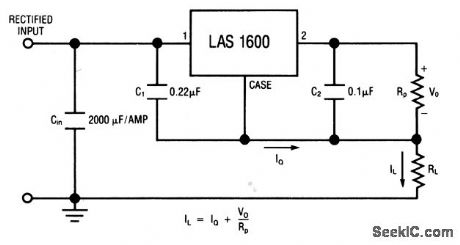
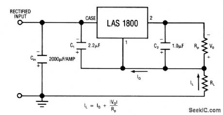
5_A_positive_fixed_current_regulator
Published:2009/7/23 23:50:00 Author:Jessie
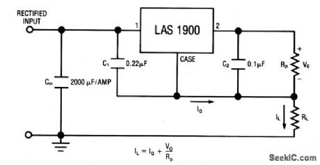
This circuit uses the LAS1900 series voltage regulator (Fig. 7-46) as a fixed-current regulator. Characteristics are shown in Fig. 7-46B, 7-46C, and 7-46D. (View)
View full Circuit Diagram | Comments | Reading(674)
5_A_positive_adjustable_voltage_regulator
Published:2009/7/23 23:50:00 Author:Jessie
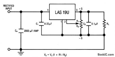
The LAS19U is a four-terminal adjustable regulator IC with an output range from +4 to +30V, providing remote sensing from a single pot. Characteristics are shown in Fig. 7-46B, 7-46C, and 7-46D. (View)
View full Circuit Diagram | Comments | Reading(861)
5_A_positive_fixed_voltage_regulator
Published:2009/7/23 23:49:00 Author:Jessie
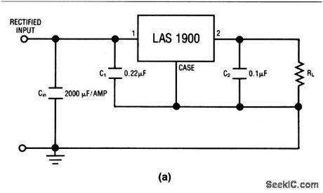
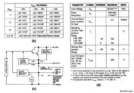
The LAS1900 series voltage regulators are ICs containing all elements necessary for linear regulation (safe area protection, thermal overload, current limiting, as shown in Fig. 7-46C). Figure 7-46B shows the output voltage and tolerance for the various LAS1900 part numbers. Figure 7-46D shows the absolute maximum ratings. (View)
View full Circuit Diagram | Comments | Reading(823)
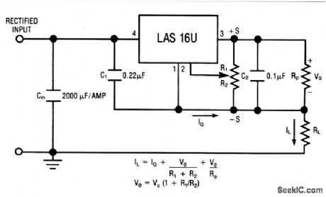
2_A_positive_adjustable_voltage_regulator
Published:2009/7/23 23:34:00 Author:Jessie
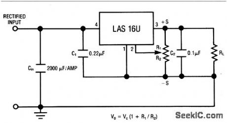
The LAS16U is a four-terminal adjustable regulator IC with an output range from +4 to+30 V, providing remote-sense capability with a single pot. Characteristics are shown in Fig.7-37B, 7-37C, and 7-37D. (View)
View full Circuit Diagram | Comments | Reading(775)
Ultra_linear_V_F_converter
Published:2009/7/23 23:34:00 Author:Jessie
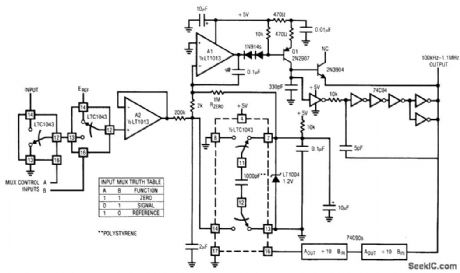
Fig. 12-10 Although this circuit can be used in a stand-alone mode, it is specifically intended for processor-driven applications, which require 17-bit accuracy, such as weighing scales. The circuit has a resolution of 1 ppm, with linearity inside 7 ppm (0.0007%). When combined with a processor-driven gain/zero calibration loop, the circuit has negligible zero and gain drift. A single 5-V supply is used to minimize interface problems. For processor operation, the input multiplexer (LTC1043) and RZERO (1 MΩ) must be added. With the multiplexer set to the ZERO function (see truth table) the A1 input is grounded, and the 200-kΩ.resistor receives no drive. However, At receives bias via RZERO and the circuit oscillates around 100 kHz. After reading this frequency, the processor shifts the multiplexer to the SIGNAL function, where the A2 output is a buffered version of the signal input. The circuit output frequency is now determined by this input, and the current through RZERO. Typical output range from 100 kHz to 1 MHz. Linear Technology. Linear Applications Handbook 1990 AN14-7. (View)
View full Circuit Diagram | Comments | Reading(740)
Sine_wave_output_V_F_converter
Published:2009/7/23 23:38:00 Author:Jessie
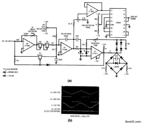
Fig. 12-12 Most of the V/F converters in this chapter produce pulse or square-wave outputs. Many applications (such as audio, filter, or automatic-equipment testing) require a sine-wave output, such as is produced by this circuit. The sine waves from this circuit span a range from 1 Hz to 100 kHz (100 dB or X5 decades) for a 0- to 10-V input, with 0.1% frequency linearity and 0.2% distortion. Drift is 150 ppm/℃ and zero-point drift is 0. 1 Hz/℃. To trim, apply 10.00 V and adjust the 2-kΩ 100-kHz distortion trim for a symmetrical triangle output at Al. Next, apply 100μV and adjust the 50-kΩ 10-Hz distortion trim for triangle symmetry. Then, apply 10.00 V again and adjust the 5-kΩ frequency trim for a 100.00-kHz output. Finally, adjust both 1-kΩ fine distortion trim potentiometers for minimum distortion of the sine-wave output (trace D of Fig. 12-12B). Slight readjustment of the other trim controls might be required to get the lowest possible distortion. (View)
View full Circuit Diagram | Comments | Reading(813)
_12_V_flash_memory_programming_supply
Published:2009/7/23 23:37:00 Author:Jessie
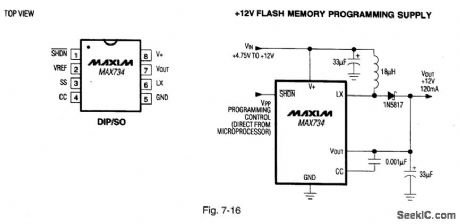
Figure 7-16 shows a MAX734 connected as a flash-memory programming supply. Typical efficiency is 85%. The IC also has a logic-controlled shutdown pin that allows direct microprocessor control. MAXIM HIGH-RELIABILITY DATA Book, 1993, P. 4-65. (View)
View full Circuit Diagram | Comments | Reading(622)
Single_cell_V_F_converter_1_Hz_to_1_kHz
Published:2009/7/23 23:35:00 Author:Jessie
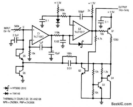
Fig. 12-11 This circuit operates from a single 1.5-Vbattery, with only 125-μA current drain, to provide a range from 1Hz to 1kHz. Drift is 250ppm/℃. Battery discharge introduces less than 1% error over 1000 hours of operation. To trim, set the input to 1.000V and adjust the 500-kΩ potentiometer for an output of 1.000 kHz. (View)
View full Circuit Diagram | Comments | Reading(858)
2_A_positive_fixed_current_regulator
Published:2009/7/23 23:34:00 Author:Jessie

This circuit uses the LAS1600 series voltage regulator (Fig. 7-37A) as a fixed-current regulator. Characteristics are shown in Fig. 7-37B, 7-37C, and 7-37D. (View)
View full Circuit Diagram | Comments | Reading(541)
1_X_transfer_function_V_P_converter_10_kHz_to_50_Hz
Published:2009/7/23 23:41:00 Author:Jessie
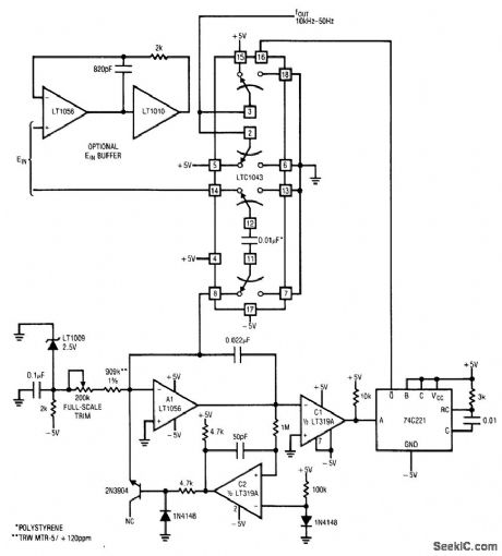
Fig. 12-14 This circuit is more accurate than that or Fig. 12-13, and it converts input voltages of 0 V to 5 V to an output frequency of 10 kHz to 50 Hz with a 0.005% accurate 1/X conformity. Drift is about 50 ppm/℃. One possible disadvantage is that this circuit draws an input current directly proportional to input voltage (to charge the LTC1043 0.01-pF capacitor). When the input voltage is 5 V, the circuit requires about 25 mA at pin 14 of the LTC1043. The optional buffer provides the necessary drive, although the input-voltage range must fall within the common-mode limits of the buffer. To trim, apply 5.000 V and adjust the full-scale trim for 50-Hz output. Linear Technology Linear Applications Handbook 1990, p. AN14-13. (View)
View full Circuit Diagram | Comments | Reading(655)
15_A_dual_adjustable_voltage_regulator
Published:2009/7/23 23:40:00 Author:Jessie
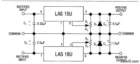
This circuit uses an LAS15U (Fig. 7-33) and an LAS18U (Fig. 7-43) to form a dual, adjustable, voltage regulator with outputs from +1.2 to +32 V and -2.6 to -30 V. The LA515U characteristics are shown in Fig. 7-32B, C and D, The LAS18U characteristics are shown in Fig. 7-42B, 7-42C, and 7-42D. (View)
View full Circuit Diagram | Comments | Reading(1106)
2_A_positive_adjustable_current_regulator
Published:2009/7/23 23:39:00 Author:Jessie
This circuit uses the LAS16U voltage-regulator IC (Fig. 7-38) as an adjustable-current regulator. Characteristics are shown in Fig. 7-37B, 7-37C, and 7-37D. (View)
View full Circuit Diagram | Comments | Reading(634)
Positi_to_negative_dc_dc_inverter
Published:2009/7/23 23:47:00 Author:Jessie
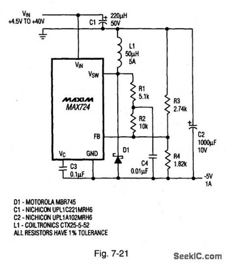
Figure 7-21 shows the MAX724 connected to provide -5 V at a 1-A output with a+4.5-V to+40-V input.See Figs.7-18 and 7-19 for pln configurations and Fig.7-20 for component suppliers,MAXIM EVALUATION KIT DATA Book,1994 P.3-138. (View)
View full Circuit Diagram | Comments | Reading(707)
15_A_negative_adjustable_current_regulator
Published:2009/7/23 23:45:00 Author:Jessie
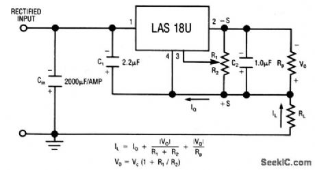
This circuit uses the LAS18U voltage-regulator IC (Fig.7-43) as an adjustable-current regulator. Characteristics are shown in Fig. 7-42B, 7-42C, and 7-42D. (View)
View full Circuit Diagram | Comments | Reading(708)
MICROPROCESSOR_POWER_SUPPLY_WATCHDOG
Published:2009/7/3 2:59:00 Author:May
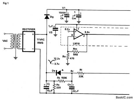
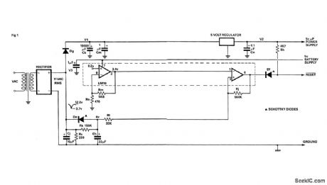
Circuit Notes
The circuit monitors the input to the microprocessor 5 V regulated supply for voltage drops and initiates a reset sequence before supply regulation is lost. In operation, the resistor capacitor combination Rs and Cj form a short time constant smoothing network for the output of the fullwave bridge rectifier. An approximately triangular, voltage waveform appears across C and Rs and it is the minimum excursion of this that initiatesthe reset. Diode Dg prevents charge sharing between capacitors Cj and Ck. Resistors Rn and Rm form a feedback network around the voltage reference section of the LM10C, setting a threshold voltage of 3.4 volts. The threshold voltage is set at 90% of the minimum voltage of the triangular waveform. When the triangular wave trough, at the comparator's non-inverting input, dips below the threshold, the comparator output is driven low. This presents a reset to the microprocessor. Capacitor Ch is charged slowly through resistor Rk and discharged rapidly through diode De. (View)
View full Circuit Diagram | Comments | Reading(695)
15_A_negative_fixed_current_regulator
Published:2009/7/23 23:44:00 Author:Jessie
This circuit uses the LAS1800 series voltage regulator (Fig. 7-42A) as a fixed-current regulator. Characteristics are shown in Fig. 7-42B, 7-42C, and 7-42D. (View)
View full Circuit Diagram | Comments | Reading(581)
| Pages:141/291 At 20141142143144145146147148149150151152153154155156157158159160Under 20 |
Circuit Categories
power supply circuit
Amplifier Circuit
Basic Circuit
LED and Light Circuit
Sensor Circuit
Signal Processing
Electrical Equipment Circuit
Control Circuit
Remote Control Circuit
A/D-D/A Converter Circuit
Audio Circuit
Measuring and Test Circuit
Communication Circuit
Computer-Related Circuit
555 Circuit
Automotive Circuit
Repairing Circuit