
Index 150
RF_bias_source
Published:2009/7/24 3:25:00 Author:Jessie
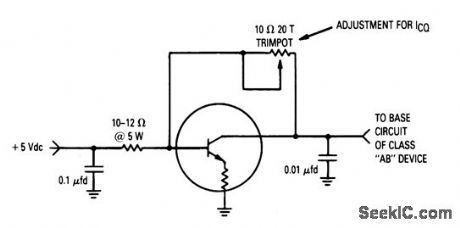
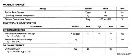
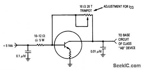
The BT500 shown in this circuit is designed for use in class-AB amplifiers to provide a thermally tracked bias source. The electrical characteristics are given in Fig. 2-44B. (View)
View full Circuit Diagram | Comments | Reading(743)
15_V_preset_output_controller
Published:2009/7/24 3:24:00 Author:Jessie
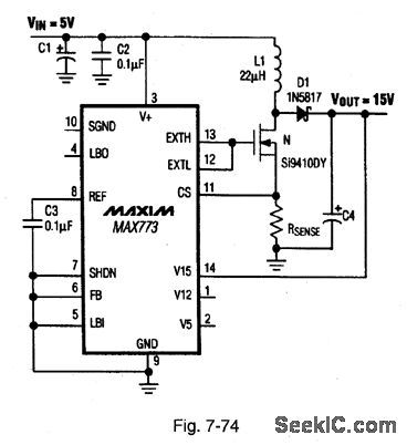
Figure 7-74 shows a MAX773 connected to provide 15-V output, with a 5-V input. This circuit is non-boot-strapped for minimum current consumption. See Fig. 7-68 for component suppliers. MAXIM NEW RELEASES DATA Book, 1995, P. 4-151. (View)
View full Circuit Diagram | Comments | Reading(703)
Nanopower_op_amp
Published:2009/7/24 3:21:00 Author:Jessie
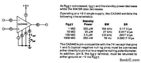
The standby-power consumption, bandwidth, and slew rate (chapter 10) of this single-supply op amp are determined by the value of RSET, as shown in the table of Fig. 8-37B. Notice that the CA3440 is pin compatible with a 741, except that pins 1 and 5 (typically negative nulling pins) must be connected either directly to pin 4 or to a negative nulling pot. Also, pin 8, the ISET terminal, must be returned to either ground or -V via RSET. (View)
View full Circuit Diagram | Comments | Reading(691)
12_V_preset_output_controller_with_power_monitor
Published:2009/7/24 3:21:00 Author:Jessie
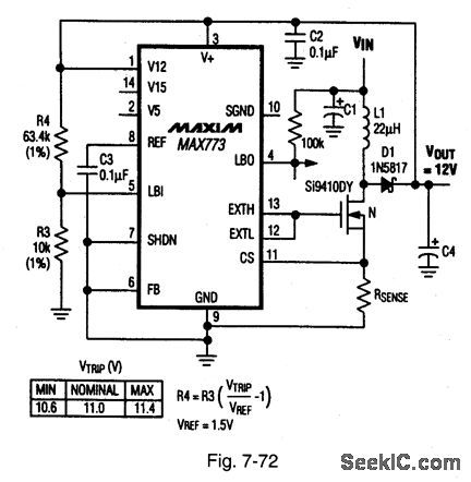
Figure 7-72 shows a MAX773 connected to provide 12-V output. with a power-monitor(or low battery )function.See Fig,7-68 for component suppliers. MAXIMNEW RELEASES DATA Book, 1995, P.4-151. (View)
View full Circuit Diagram | Comments | Reading(716)
Two_cell_voltmeter_with_high_input_resistance
Published:2009/7/24 3:18:00 Author:Jessie
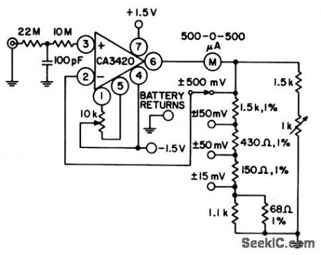
This two-cell voltmeter has an input resistance in excess of 1,000,000 MΩ. Full-scale deflection is ±500 mV, ±150 mV, and ±15 mV. Higher voltage ranges can be added with external input-voltage attenuator networks. The meter is in series with the gain network, thus eliminating the meter temperature-coefficient error term. Standby supply current (meter not deflected) is 300 μA. At full-scale deflection, current rises to 800 μA. Carbon-zinc battery life should be in excess of 1000 hours. (View)
View full Circuit Diagram | Comments | Reading(636)
Two_cell_picoammeter
Published:2009/7/24 3:18:00 Author:Jessie
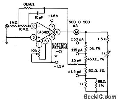
This circuit covers the range from ±1.5 pA to ±500 μA. Higher current ranges are possible with suitable switching techniques and scaling resistors. The 1-MΩ input resistor provides input-transient protection. Higher current ranges require that this resistor be reduced. The 10-MΩ resistor at pin 2 decouples possible high input capacitance, and reduces the tendency for the circuit to oscillate. (View)
View full Circuit Diagram | Comments | Reading(1737)
9_V_high_efficiency_controller_lower_power
Published:2009/7/24 3:17:00 Author:Jessie
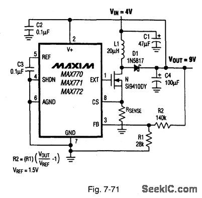
Figure 7-71 shows the MAX770/71/72 connected to provide 9-V output with a 4-V input. See Fig. 7-68 for component suppliers. These IC controllers are similar to the MAX1771 (Fig. 7-53), but with lower power capability. MAXIM NEW RELEASES DATA BOOk, 1995, P. 4-150. (View)
View full Circuit Diagram | Comments | Reading(642)
SERIES_REGULATED_LINEAR_POWER_SUPPLY
Published:2009/7/24 3:37:00 Author:Jessie
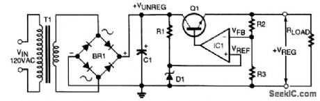
The ac line is isolated from the power supply by transformer T1. Full-wave diode bridge BR1 de-livers unregulated dc with ripple on it to the filter capacitor (C1.) The filtered dc is delivered to pass transistor Q1, shown here in series with the load. The series-pass regulator with a transistor pass element regulates the voltage to ensure that a constant output level is maintained, despite variations in the power line voltage or circuit loading. The basic linear series regulator consists of transistor Q1, reference resistor R1, sensing resistors R2 and R3, voltage-reference zener diode D1, and operational amplifier IC1, organized as an error amplifier The zener diode D1 provides a fixed reference voltage at the positive input to amplifier IC1. The output voltage of the supply establishes the emitter volt-age and provides a feedback voltage for the negative terminal of the amplifier IC1, The equation for the regulated output voltage is Vreg=Vref(1+R1/R2) (View)
View full Circuit Diagram | Comments | Reading(1065)
Micropowover_inverting_switching_regulator
Published:2009/7/24 3:37:00 Author:Jessie
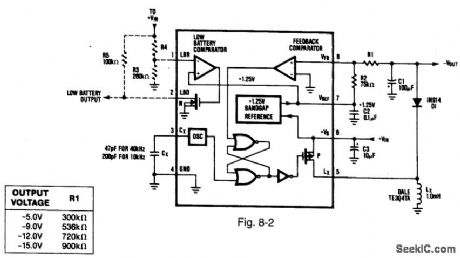
Figure 8-2 shows a MAX634 connected to provide -5-V, -9-V, -12-V, or -15-V outputs, depending on the value of R1. Figure 8-3 shows coil and core manufacturers. The input can be from +3V to +16.5 V, with 100 μA typical operating current and 85% efficiency. Nhxttvt NEW RELEASES DATA BOOK, 1992, P. 4-69, 4-70. (View)
View full Circuit Diagram | Comments | Reading(732)
Low_voltage_step_up_converter
Published:2009/7/24 3:37:00 Author:Jessie
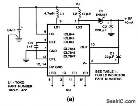
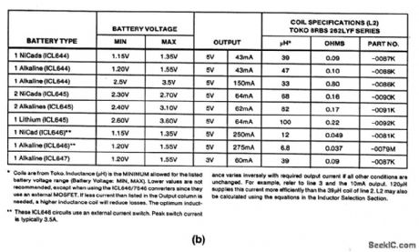
This circuit shows a switching converter (chapter 4) that provides +5 V at 40 mA from one or two battery cells. Figure 8-42B shows the L2 inductor part numbers for a number of readily available batteries. (View)
View full Circuit Diagram | Comments | Reading(673)
LOW_OUTPUT_FOR_POWER_ON
Published:2009/7/1 20:28:00 Author:May
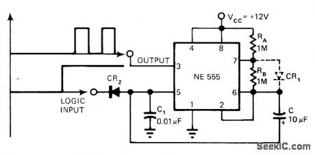
Logic signal controls both turn-on and turnoff of 555 timer used as oscillator. When input signal at cathode of CR2 goes low, oscillator remains off and out-put at pin 3 is low. When input goes high, os-cillator starts with its first state low so there are no initial pulse errors.-K. D. Dighe, Rearranged Components Cut 555's Initial-Pulse Errors, EDN Magazine, Jan. 5, 1978, p 82 and 84 (View)
View full Circuit Diagram | Comments | Reading(641)
Micropower_step_up_switching_regulator
Published:2009/7/24 3:35:00 Author:Jessie

Figure 8-1 shows a MAX630 connected to provide -15-V output at 20 mA. The input can be from 2.0 V to 16.5 V, with 70-μA typical operating current, 1-μA maximum quiescent current, and a 85% (typical) efficiency. MAXIM NEW RELEASES DATA Book, 1992, P. 4-49. (View)
View full Circuit Diagram | Comments | Reading(670)
Basic_meter_amplifier
Published:2009/7/24 3:30:00 Author:Jessie
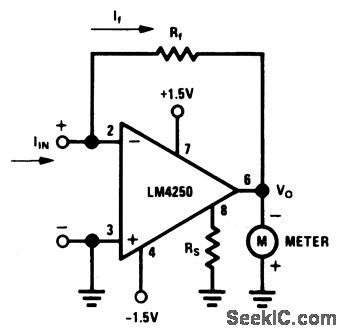
This circuit operates from two D cells, and provides a current range as low as 100 nA full-scale. With RS set at 10 MΩ, the total current drain is 0.6 μA for a total power-supply drain of 1.8 μW. Input bias current is about 600 pA. When operated with two No. 950 D cells (Eveready), quiescent power drain is so low that no on/off switch is needed (typically, batteries last for a minimum of one year).Meter deflection is set by the value of Rf, where output voltage VO, equals If/Rf. A practical value for full-scale meter deflection is 300 mV. (View)
View full Circuit Diagram | Comments | Reading(699)
135_VDC_SUPPLY
Published:2009/7/24 3:28:00 Author:Jessie
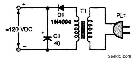
This supply can be used for vacuum-tube experiments. It uses a 120:120 Vac isolation trans-former to isolate the ac line from the dc output. T1 can be 30- to 100-mA capacity and C1 is a 40-μF 250-V electrolytic. (View)
View full Circuit Diagram | Comments | Reading(754)
500_nW_x_10_amplifier
Published:2009/7/24 3:28:00 Author:Jessie
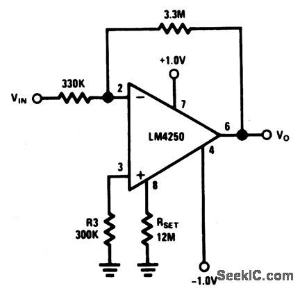
This circuit has a quiescent power dissipation of 470 nW, with a slew rate of 1 V/ms for a 0.05-μA set current. The 3-dB down (gain of -7.07) frequency for the circuit is about 300 Hz. Peak-to-peak output swing into a 100-kΩ load is 0.7 V or ±0.35 V peak. An increase in supply voltage to ±1.35 V (such as two mercury cells) increases the output swing by ±0.35 V to 1.4 V peak-to-peak. This increases the power dissipation to about 1 μW per cell, a power drain of 15 μW or less will not affect the shelf life of a mercury cell. (View)
View full Circuit Diagram | Comments | Reading(756)
RE_bias_source_SOE_style_tpacknge
Published:2009/7/24 3:28:00 Author:Jessie
The BT500F shown in this circuit is designed for use in class-AB amplifiers to provide a thermally tracked bias source. The electrical characteristics are given in Fig. 2-45B. (View)
View full Circuit Diagram | Comments | Reading(629)
16_V_preset_output_controller
Published:2009/7/24 3:27:00 Author:Jessie
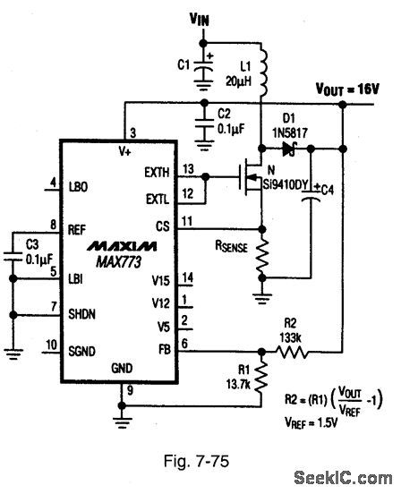
Figure 7-75 shows a MAX773 connected to provide 16-V output, with a 5-V input. This circuit is boot-strapped for operation with inputs less than 5 V. See Fig. 7-68 for component suppliers. MAXIM NEW RELEASES DATA Book, 1995, P. 4-15t. (View)
View full Circuit Diagram | Comments | Reading(601)
Three_terminal_regulation_with_remote_sensing
Published:2009/7/24 4:51:00 Author:Jessie

This circuit allows the regulator to remotely sense the feedback voltage and eliminate the effects of voltage drop in the supply lines. This is useful where high currents must be transmitted over relatively long supply lines or PC rails. A1 senses the voltage at the point of load. The A1 output, summed with the regulator output, modifies the adjustment pin voltage to compensate for the voltage lost across RDROP. The feedback divider is returned through a separate lead from the load. (View)
View full Circuit Diagram | Comments | Reading(795)
Zero_crossing_detector_single_supply
Published:2009/7/24 4:48:00 Author:Jessie
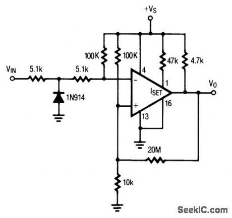
Fig. 15-29 This circuit is similar to that of Figs. 15-2, 15-7, 15-9, 15-15, and 15-17, but it uses only one section of an LP165/365 and it requires a single supply. Figures 15-24B and 15-24C show the pin connections and electrical characteristics, respectively. Raytheon Linear Integrated Circuits, 1989, p. 5-40. (View)
View full Circuit Diagram | Comments | Reading(893)
Increasing_three_terminal_regulator_stability
Published:2009/7/24 4:47:00 Author:Jessie
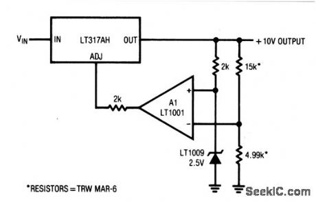
This circuit shows a way to increase the stability of regulator output over time and temperature. The circuit is particularly useful in powering strain-gauge transducers (chapter 14). The output voltage is divided down and compared to the 2.5-V reference by A1, which, in turn, forces the adjustment pin to whatever voltage is required to maintain the 10-V output. (View)
View full Circuit Diagram | Comments | Reading(714)
| Pages:150/291 At 20141142143144145146147148149150151152153154155156157158159160Under 20 |
Circuit Categories
power supply circuit
Amplifier Circuit
Basic Circuit
LED and Light Circuit
Sensor Circuit
Signal Processing
Electrical Equipment Circuit
Control Circuit
Remote Control Circuit
A/D-D/A Converter Circuit
Audio Circuit
Measuring and Test Circuit
Communication Circuit
Computer-Related Circuit
555 Circuit
Automotive Circuit
Repairing Circuit