
Index 157
Low_cost_buck_regulator
Published:2009/7/24 5:44:00 Author:Jessie
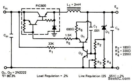
This low-cost circuit provides line regulation (at a value set by D1) with a minimum of components. Typical values for Cin, and Co are 500μF. (View)
View full Circuit Diagram | Comments | Reading(895)
Boost_switching_regulator
Published:2009/7/24 5:43:00 Author:Jessie
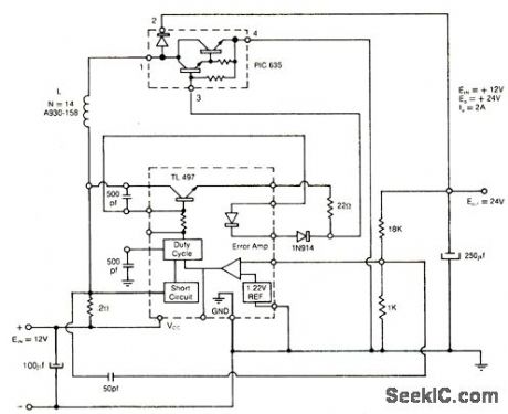
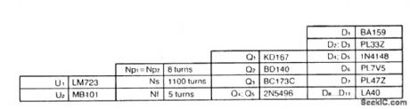
This circuit provides an output (+24 V) that is double the input (+ 12 V). (View)
View full Circuit Diagram | Comments | Reading(937)
Negative_voltage_flyback_regulator
Published:2009/7/24 5:42:00 Author:Jessie
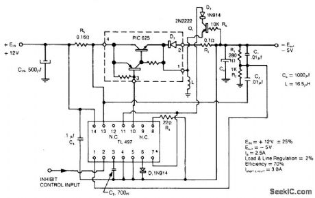
This circuit provides a negative output (-5 V) with a positive input (+12 V). (View)
View full Circuit Diagram | Comments | Reading(874)
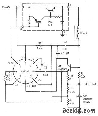
High_voltage_negative_switching_regulator
Published:2009/7/24 5:41:00 Author:Jessie
The characteristics of this circuit are the same as in Fig, 4-26, except that the input can exceed 40 V, and the input/output is negative. (View)
View full Circuit Diagram | Comments | Reading(676)
High_voltage_positive_switching_regulator
Published:2009/7/24 5:39:00 Author:Jessie
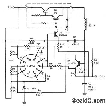
The characteristics of this circuit are the same as in Fig. 4-26, except that the input can exceed 40 V. (View)
View full Circuit Diagram | Comments | Reading(640)
Alternate_positive_voltage_switching_regulator
Published:2009/7/24 5:38:00 Author:Jessie
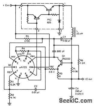
The input and output characteristics of this circuit are the same as in Fig. 4-26, except that a μA723 is used instead of an LM305. Notice that a 2N2222 is required for Q 1 . (View)
View full Circuit Diagram | Comments | Reading(507)
Negative_voltage_switching_regulator
Published:2009/7/24 5:36:00 Author:Jessie
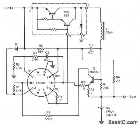
The input and output characteristics of this circuit are the same as in Fig. 4-26, except that input and output are negative. (View)
View full Circuit Diagram | Comments | Reading(706)
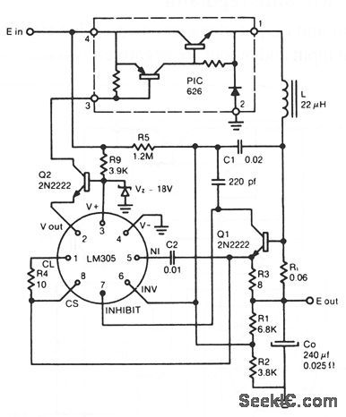
Positive_voltage_switching_regulator
Published:2009/7/24 5:35:00 Author:Jessie
With the values shown, this circuit produces a±5-V output (± 1%), with a 20- to 40-V input, at currents between 2 and 10 A. mVpp (View)
View full Circuit Diagram | Comments | Reading(707)
Dc_dc_converter_without_external_sync
Published:2009/7/24 5:34:00 Author:Jessie
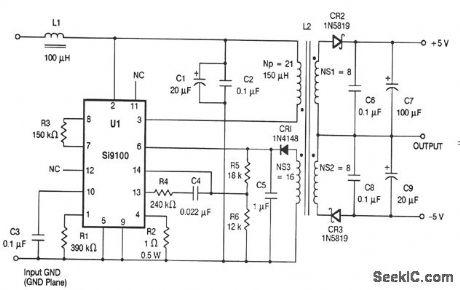
This circuit is similar to that of Figs. 4-22 and 4-24, except that there is no provision for extenal sync. The input voltage is 15 to 70 V. Typical maximum loads are 167 mA at +5V, and 33 mA at -5V. Typical minimum loads are 32 mA at + 5 V and 8 mA at -5 V. Maximum ripple is 100 mVpp. Regulation is ±5%. L1 is any 100-μH 75-mA inductor. L2 is GFS Manufacturing #85-787-4. (View)
View full Circuit Diagram | Comments | Reading(841)
WARNING_LIGHT_OPERATES_FROM_BATTERY_POWER_SUPPLY
Published:2009/6/30 23:50:00 Author:May
The circuit provides illumination when darkness comes. By using the gain available in darlington transistors, this circuit is simplified to use just a photodarlington sensor, a darlington amplifier, and three resistors. The illumination level will be slightly lower than normal, and longer bulb life can be expected, since the D40K saturation voltage lowers the lamp operating voltage slightly. (View)
View full Circuit Diagram | Comments | Reading(1001)
+5_to__24_V_at_40_mA(with_low_power)inverter
Published:2009/7/24 9:03:00 Author:Jessie
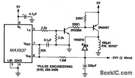
This circuit is similar to that of Fig,4-60 In that the 2N4407 is a buffered replica of the MAX637 LX output.However,the 2N4407 has a high breakdown voltage and can be used to generate a-24-V output.The -24-V output does not appear directly on any pin of the MAX637 because it is sensed via the 1.5-MΩ external feedback resistor . (View)
View full Circuit Diagram | Comments | Reading(814)
Step_up_down_dc_dc_converter
Published:2009/7/24 8:52:00 Author:Jessie
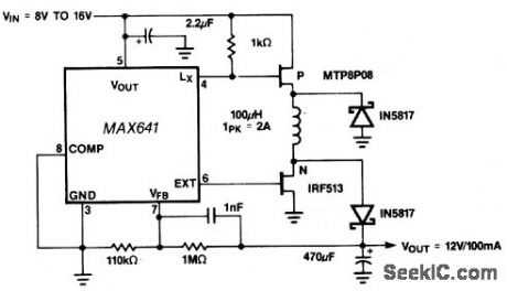
Positive-output step-up and step-down dc/dc converters have a common limitation in that neither can handle input voltages that can be both greater than (or less than) the output. For example, when convening a 12-V sealed lead-acid battery to a regulated + 12-V output, the battery voltage can vary from a high of 15 to 10 V. By using a MAX641 to drive separate P- and N-channel MOSFETs, both ends of the inductor are switched to allow noninverting buck/boost operation. A second advantage of the circuit over most boost-only designs is that the output goes to 0 V when Shutdown is activated. A drawback is that efficiency is not optimum because the two MOSFETs and diodes increase losses in the charge and discharge path of the inductor. The circuit delivers + 12 V at 100 mA with an 8-V input (70% efficiency). (View)
View full Circuit Diagram | Comments | Reading(1800)
Low_voltage_battery_to__5_V
Published:2009/7/24 8:50:00 Author:Jessie
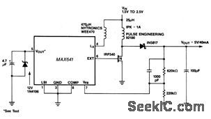
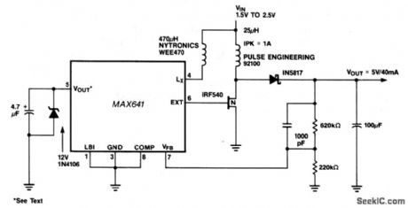

By connecting a second inductor to the LX output of a MAX641 step-up dc/dc converter, the efficiency and power-handling ability can be dramatically improved. This circuit can supply 5 V at 40 mA with only 1.5-V input. With 2.4-V input, the circuit can supply 180 mA at 5 V. Notice that VOUT is not an output (in this circuit), but is the MAX641 voltage input. The pin is so labeled because VOUT is usually the output/feedback terminal of a stand-alone MAX641. (View)
View full Circuit Diagram | Comments | Reading(820)
High_voltage_step_up_converter
Published:2009/7/24 8:49:00 Author:Jessie
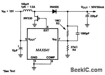
In this circuit, a +12-V input is converted to a +50 V at 50 mA by adding an IRF530 N-channel FET, which has a voltage rating of 100 V. The circuit differs from the basic MAX641 hookup in that an external resistor-divider must provide the feedback to the VFB input and that chip power comes from the + 12-V input via the VOUT pin. (View)
View full Circuit Diagram | Comments | Reading(1895)
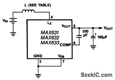
Medium_power_step_up_converters
Published:2009/7/24 8:47:00 Author:Jessie
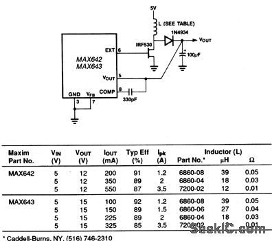
The table of Fig. 4-53B lists measured efficiency of circuits using the indicated coils. In selecting coils for circuits that use external MOSFETs, it is important to calculate the peak current and to select a coil that will not saturate at that peak current. (View)
View full Circuit Diagram | Comments | Reading(1080)
Low_power_step_up_converters
Published:2009/7/24 8:46:00 Author:Jessie
The table of Fig. 4-52B lists the measured efficiency of circuits using the indicated coils. Efficiencies can be improved slightly by placing a Schottky diode (such as the 1N5817) in parallel with the intemal diode, from pin 4 to 5. The increase in efficiency is most noticeable for the 5-V output circuits. (View)
View full Circuit Diagram | Comments | Reading(747)
_5V_from_a_3_V_battery_with_no_inductors
Published:2009/7/24 8:44:00 Author:Jessie
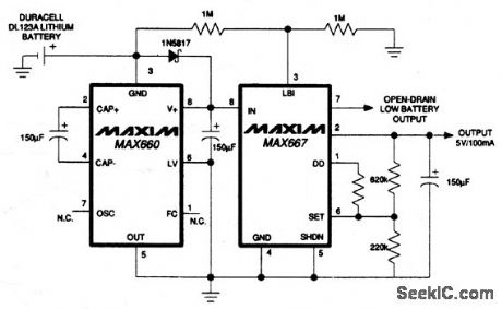
This inductorless dc/dc converter generates a regulated +5 V at up to 100 mA from a single lithium cell. When powered by a DL123A (smaller than an AA cell), the circuit provides 40 mA of load current for 12 hours or more. The MAX660 in a doubler configuration steps up the battery voltage to +6 V, which is then regulated down to + 5 V by the MAX667. The surface-mount version of this circuit occupies only 1/2 square inches of PC-board space, because the circuit uses capacitors instead of inductors. The circuit capitalizes on the low dropout voltage of the MAX667 (typically less than 100 mV at 150 mA) and the 100-mA load capability and 95% efficiency of the MAX660. (View)
View full Circuit Diagram | Comments | Reading(697)
Charge_pump_with_shutdown
Published:2009/7/24 8:43:00 Author:Jessie
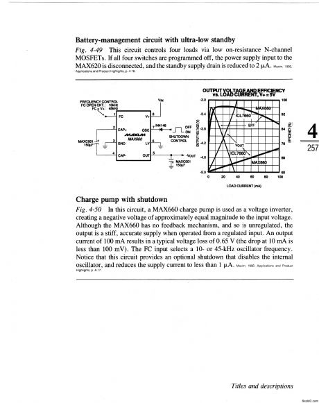
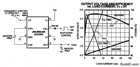
In this circuit, a MAX660 charge pump is used as a voltage inverter, creating a negative voltage of approximately equal magnitude to the input voltage. Although the MAX660 has no feedback mechanism, and so is unregulated, the output is a stiff, accurate supply when operated from a regulated input. An output current of 100 mA results in a typical voltage loss of 0.65 V (the drop at 10 mA is less than 100 mV). The FC input selects a 10- or 45-kHz oscillator frequency. Notice that this circuit provides an optional shutdown that disables the internal oscillator, and reduces the supply current to less than 1μA. (View)
View full Circuit Diagram | Comments | Reading(726)
Battery_management_circuit_with_ultra_low_standby
Published:2009/7/24 8:41:00 Author:Jessie
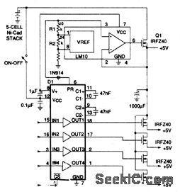
This circuit controls four loads via low on-resistance N-channel MOSFETs. If all four switches are programmed off, the power supply input to the MAX620 is disconnected, and the standby supply drain is reduced to 2μA. (View)
View full Circuit Diagram | Comments | Reading(903)
STABILIZING_A_LASER_DISCHARGE_CURRENT
Published:2009/6/30 23:39:00 Author:May
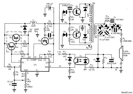
The circuit uses a free-running push-pull dc to dc high voltage converter to get the necessary voltage for the laser plasma tube supply. The supply voltage VC of this converter, is adjusted by a switch-mode power supply in order to keep the load current constant, at set value. The linear opto-electronic isolator U2, connected in series with the laser plasma tube, gives a voltage VF proportional to the discharge current ID across R18, having the correct polarity to drive directly the inverting input of U1, D7, R15 protects the optoisolator diode against damage produced by the high voltage ignition pulse.Due to the high operating frequency of the high voltage converter (25 kHz) the ripple of the laser output power is less than 2.10-4. The stability of ID is better than 10-2, for variations of supply voltage VS is the range of ±10%, and depends on the optoisolator sensitivity. (View)
View full Circuit Diagram | Comments | Reading(1664)
| Pages:157/291 At 20141142143144145146147148149150151152153154155156157158159160Under 20 |
Circuit Categories
power supply circuit
Amplifier Circuit
Basic Circuit
LED and Light Circuit
Sensor Circuit
Signal Processing
Electrical Equipment Circuit
Control Circuit
Remote Control Circuit
A/D-D/A Converter Circuit
Audio Circuit
Measuring and Test Circuit
Communication Circuit
Computer-Related Circuit
555 Circuit
Automotive Circuit
Repairing Circuit