
Index 144
DIFFERENTIAL_VOLTMETER
Published:2009/7/24 1:34:00 Author:Jessie

High-impedance differential-input transistorized panel voltmeter has stable zero point, eliminating need for undesirable zero control. Meter com pares voltage under test with known zener regulated reference voltage. Circuit is differential Darlington connected emitter-follower using pair of 2N2060's. Bias point is stabilized by constant-current sync connected to 2N1613 transistor. Accuracy is 1% if unmatched source impedance is less then 10K.-A High-Stability Differential Voltmeter, Electronic Circuit Design Handbook, Mactier Pub, Corp., N.Y., 1965, p 152. (View)
View full Circuit Diagram | Comments | Reading(1521)
DUAL_RANGE_D_C_VOLTMETER
Published:2009/7/24 1:33:00 Author:Jessie
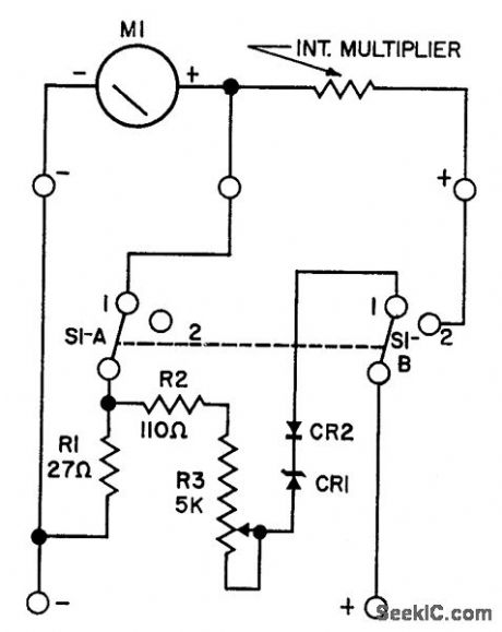
With switch in position 2, serves as standard 0-50 v d-c voltmeter. With switch in position 1, R1 is shunted across 50-my, 1-mc meter to allow about 3 ma through 27+, 1-w tenor diode CR1-CR2 diode 1N540 is for temperature compensation. About 27 v is then held across the diodes, and meter scale represents 27 to 32 v, with sensitivity of 0.1 v d-c per division. R3 is used for calibration.-M. W. Raybin, Dual Range DC Voltmeter, EEE, 10:12,p 31. (View)
View full Circuit Diagram | Comments | Reading(673)
R_F_VOLTMETER
Published:2009/7/24 1:32:00 Author:Jessie

Circuit generates low-frequency waveform whose amplitude is equivalent to that of unknown r-f voltage, using photochopper modulator VI-V2 as error detector. Arrangement gives seven voltage ranger from 10 my rms to 10 v rms full scale, over frequency range of 500 kc to 1,000 Mc.-T. C. Anderson, Measuring Low-Level R-F Voltage with Servo Feedback Techniques, Electronics, 34:28, p 63-65. (View)
View full Circuit Diagram | Comments | Reading(942)
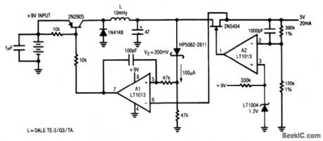
Low_power_switching_regulator
Published:2009/7/24 0:30:00 Author:Jessie
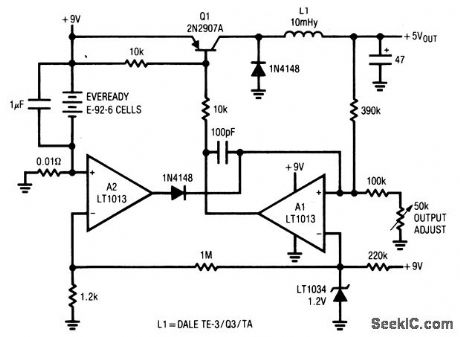
This circuit provides 5-V output from a 9-V source with 80% efficiency and 50-mA output capability. The circuit is short-circuit protected. (View)
View full Circuit Diagram | Comments | Reading(602)
Low_dropout_regulator
Published:2009/7/24 0:29:00 Author:Jessie
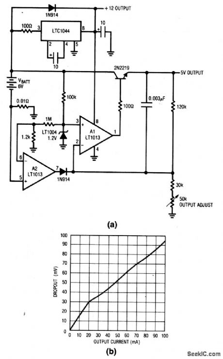
This circuit provides both a +12-V and a +5-V output from a single 6-V battery, with very low dropout (Fig.8-3B). Quiescent current is 760 μA, and the100-mA output is short-circuit protected (see chapter 4 for testing). (View)
View full Circuit Diagram | Comments | Reading(1391)
High_current_battery_splitter
Published:2009/7/24 0:27:00 Author:Jessie
This circuit can source or sink up to ±150 mA with only 5 mA quiescent current. The value of C2 can be increased as necessary to absorb current transients. (View)
View full Circuit Diagram | Comments | Reading(643)
Micropower_battery_splitter
Published:2009/7/24 0:26:00 Author:Jessie
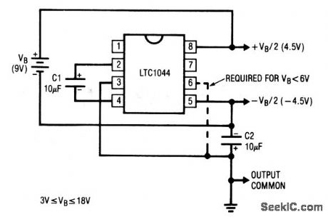
This circuit provides symmetrical ±output voltages, both equal to one-half the input voltage (one 9-V battery in this case). The output voltages are referenced to pin 3 (output common). The circuit will operate with other battery voltages. If the battery exceeds 6 V, pin 6 should also be connected to pin 3, as shown by the dashed line. (View)
View full Circuit Diagram | Comments | Reading(675)
Improved_three_terminal_regulator_for_high_voltages
Published:2009/7/24 0:22:00 Author:Jessie

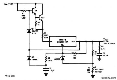
This circuit is an improved version of the circuit in Fig. 7-67. (View)
View full Circuit Diagram | Comments | Reading(647)
Lozu_dropout_P_channel_linear_regulator
Published:2009/7/24 1:30:00 Author:Jessie
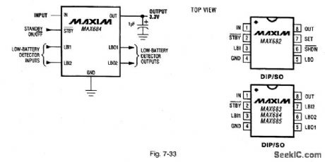
Figure 7-33 show a MAX684 linear regulator. The output voltages are: MAX682 3.3 V, MAX683 5.0 V, MAX684 3.3 V, and MAX685 3.0 V. The supply range is 2.7 V to 11.5 V, the maximum dropout is 300 mV at 200 mA output, the maximum quiescent current is 15 μA, the shutdown current is 1 μA (maximum). MAXIM NEW RELEASES DATA BOOK. 1994. P. 4-49.
(View)
View full Circuit Diagram | Comments | Reading(546)
FET_PNP_D_C_MILLIVOLTMETER
Published:2009/7/24 1:29:00 Author:Jessie
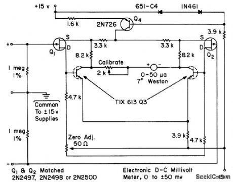
Differential amplifier uses pair of simple feedback amplifiers having voltage gain of 3, output impedance of 50K, input sensitivity of 20. meg/v, and common mode rejection ratio of 1,000 to 1.-Texas Instruments Inc., Solid-State Communications, McGraw-Hill, N.Y., 1966, p 136. (View)
View full Circuit Diagram | Comments | Reading(696)
Charge_pump_voltage_converter
Published:2009/7/24 1:28:00 Author:Jessie
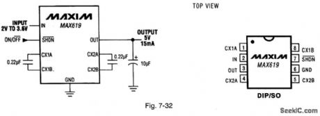
Figure 7-32 shows a MAX619 connected to provide a 5-V, 15-mA output, with 2-V to 3.6-V input, using two inexpensive capacitors, The quiescent current is 150 μA (max) with 10μA (max) shutdown current. MAXIM NEw RELEAsEs DATA BOOK, 1994, P. 4-37.
(View)
View full Circuit Diagram | Comments | Reading(693)
High_speed6_A_single_MOSFET_drivers
Published:2009/7/24 1:26:00 Author:Jessie
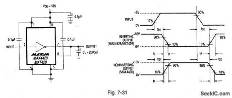
Figure 7-30 shows the MAX4429/MXT429 connected to translate TTL/CMOSinputs to high-voltage/high-current outputs,The output impedance is 1.5 Ω witha 6-A current.Delay time is 40 ns, with 25-ns rise/fall times(into a 2500-pF load).Figure 7-31 shows the timing test circuit.The supply range is 4.5 V to 18 V,with anoutput swing to within 25 mV of VDD and ground.MAXIM NEW RELEASES DATABook,1994, P.4-31.4-35, (View)
View full Circuit Diagram | Comments | Reading(728)
Ratio_V_F_converter
Published:2009/7/24 1:14:00 Author:Jessie
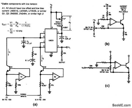
Fig. 12-25 This circuit converts the ratio of two voltages to an equivalent frequency (essentially the same function as performed by the circuit of Fig. 12-16). In this circuit, the two op amps convert the inputs to proportional currents. The 1-kΩ scale-factor trim is adjusted so that the frequency output equals the ratio of V1/V2 x 10 kHz. Full-scale output is 15 kHz. The circuit can accept positive inputs when the op-amps are rearranged, as shown in Figs. 12-25B or 12-25C. Trimming out the offset in the Op amp gives the ratio converter better linearity and accuracy, e trim circuit Fig. 12-25B needs stable positive and negative supplies for the offset trimmer, but the trim In Fig, -25C needs only an astable positive supply. Unmarked components in Fig. 12-25C are the same as those in Fig. -25B. (View)
View full Circuit Diagram | Comments | Reading(744)
Simple_voltage_doubler
Published:2009/7/24 0:34:00 Author:Jessie
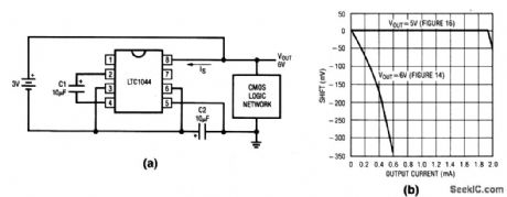
This circuit doubles available battery voltage using an LTC1044 switched-capacitor voltage converter. The circuit will drive low-power 74-CMOS (3-to 15-V) equipment for extended periods of time from two small 1.5-V cells. Efficiency exceeds 90% for load currents below 1.75 mA. Figure 8-7B shows output voltage versus loading (shown as VOUT=6 V). (View)
View full Circuit Diagram | Comments | Reading(822)
Inductorless_high_current_switching_regulator
Published:2009/7/24 0:33:00 Author:Jessie
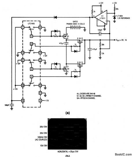
This circuit operates from 12-V battery (6 cells), and provides5-V output at 1 A. Notice that no inductor is required. (View)
View full Circuit Diagram | Comments | Reading(627)
Switching_preregulated_linear_regulator_low_noise
Published:2009/7/24 0:31:00 Author:Jessie
This circuit is similar to that of Fig. 8-4, except that the low-dropout series regulator at switching-regulator output serves to eliminate switching-induced noise. The circuit also operates from a 9-V battery and will supply 25-mA of noise-free, regulated power with short-circuit current set by the FET 30-mA IDSS. (View)
View full Circuit Diagram | Comments | Reading(1033)
LOW_DISSIPATION_1_MC_FLIP_FLOP
Published:2009/7/24 1:42:00 Author:Jessie
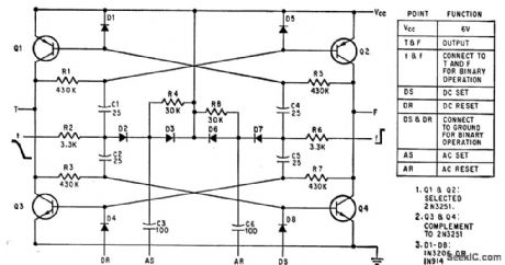
Complementary-pair circuit keeps power dissipation below 2 mw, with standby power of only 150 microwatts. Consists of two interconnected flip-lops, sharing common diode steering network at input. Diodes D1, D4, D5, and D8 protect emitter-based junctions from breakdown and also increase switching speed by clamping back bias levels at base of transistor. May be used for binary operation, as staler, or as shift register.-M. E. McGee and J. H. Wujek Jr., One-Megahertz Flip-Flop Saves Standby Power, Electronics, 39:12, p 106-107. (View)
View full Circuit Diagram | Comments | Reading(792)
Current_mode_SMPS_controllers
Published:2009/7/24 1:41:00 Author:Jessie

Figure 7-40 shows the MAX741D connected to provide +5 V at 1.5 A or 3.0 A with a 6-V to 15.5-V input. Figure 7-41 shows the MAX741D connected to provide +5 V at 1 A from a +3-V input. Both configurations are SMPS (switch-mode power supplies). The data sheet shows how the MAX741 can be programmed to provide different outputs with supply voltages from 2.7 V. MAXIM NEW RELEASES DATA Book, 1994, P. 4-131. (View)
View full Circuit Diagram | Comments | Reading(858)
HIGH_IMPEDANCE_DIFFERENTIAL_VTVM
Published:2009/7/24 1:41:00 Author:Jessie

Infinite input impedance is obtained in direct.coupled d-c amplifier by continuously and automatically feeding back to input a bucking voltage equal to signal voltage. Use of both inputs permits differential easurements of small signal voltages at mean levels between -150 and +300 v, for measuring grid-cathode potentials in high-impedance circuits or for balancing high-impedance push-pull circuits. Instead of input voltage dividers, range resistors are used in output circuit. Voltage supply need not be regulated.-V. D. Schurr, D-C Amplifier Expands Input Voltage Range, Electronics, 31:23, p 87-89. (View)
View full Circuit Diagram | Comments | Reading(548)
SCR_AND_LAMP_DISPLAY_CONTENTS_OF_REGISTER
Published:2009/7/24 1:40:00 Author:Jessie
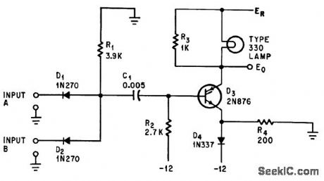
Computer register lo be sampled is connected to input A, and input B is fed with 10-microsec, 12-V positive pulse. When output of register is at its low level of -12 V, diode D1 conducts but D2 does not, so scr D3 is nonconducting and lamp is off. When register output is high level (ground potential), coincident positive voltages applied to base of scr make it conduct and turn lamp on. -J. J. Collins, Displaying the Contents of a Computer Register, Electronics, 37:21, p 72. (View)
View full Circuit Diagram | Comments | Reading(698)
| Pages:144/291 At 20141142143144145146147148149150151152153154155156157158159160Under 20 |
Circuit Categories
power supply circuit
Amplifier Circuit
Basic Circuit
LED and Light Circuit
Sensor Circuit
Signal Processing
Electrical Equipment Circuit
Control Circuit
Remote Control Circuit
A/D-D/A Converter Circuit
Audio Circuit
Measuring and Test Circuit
Communication Circuit
Computer-Related Circuit
555 Circuit
Automotive Circuit
Repairing Circuit