
Index 161
Voltage_comparator_with_DTL_TTL_output
Published:2009/7/24 21:30:00 Author:Jessie
This circuit converts small differential-input signals into levels suitable to drive DTL/TTL loads. (View)
View full Circuit Diagram | Comments | Reading(709)
33_5_V_12_V_and__18_V_from_two_to_three_cells
Published:2009/7/24 23:19:00 Author:Jessie
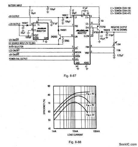
Figure 8-87 shows a MAX722 palmtop SMPS (surface-mount power supply), and a MAX734 regulator connected to provide a main 3.3-V/5-V output, a +12-V output for flash programming, and a -18-V output for LCD bias-all with a 1.8-V to 5.5-V input range. Quiescent current (when VIN = 3 V, and the 12-V line is off) is 350 μA. With a VIN of 2 V, the maximum load capability for the 5-V output is 200 mA, and the +12-V output, 40 mA. When VIN is increased to 2.5 V, the 5-V output provides 275 mA, and the +12-V output, 60 mA. Figure 8-88 shows the efficiency curves for the + 12-V output. If the main output is set at 3.3 V (pin 3 of the MAX722 high), connect the MAX734 V + pin to +12 V (instead of +5 V, as shown) to get the extra gate drive for the MAX734 MOSFET. MAXIM BATTERY MANAGEMENT CIRCUIT COLLECTION, 1994, P. 12. (View)
View full Circuit Diagram | Comments | Reading(639)
NICAD_CHARGER_FOR_AUTO
Published:2009/6/29 21:35:00 Author:May
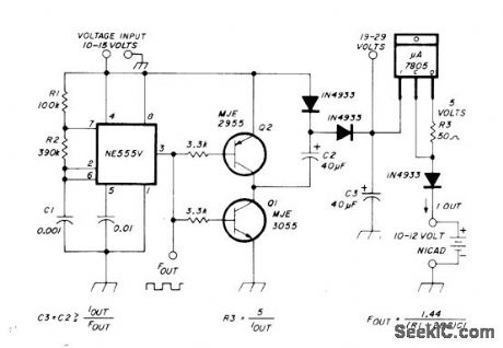
Voltage doubler provides at least 20 V from 12-V auto battery, for constant-current charging of 12-V nicads, using NE555 timer and two power transistors. Doubled voltage drives source current into three-terminal current regulator. Switching frequency of NE555 as MVBR is 1.4 kHz. Charging currentis set at 50 mA for charging ten 500-mAh nicads.-G. Hinkle, Constant-Current Battery Charger for Portable Operation, Ham Radio, April 1978, p 34-36. (View)
View full Circuit Diagram | Comments | Reading(2031)
NICAD_ZAPPER
Published:2009/6/29 21:33:00 Author:May
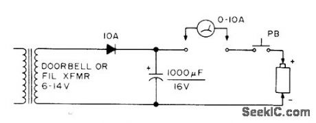
Simple circuit often restores dead or defective nicad battery by applying DC overvoltage at current up to 10 A for about 3 s. Longer treatment may overheat battery and make it explode.-Circuits, 73 Magazine, July 1977,p 35. (View)
View full Circuit Diagram | Comments | Reading(1203)
LED_TRICKLE_CHARGER
Published:2009/6/29 21:32:00 Author:May
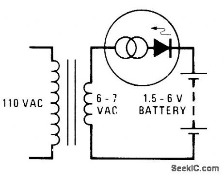
Constant-current characteristic of National NSL4944 LED is used to advantage in simple half-wave charger for batteries up to 6 V.- Linear Applications, Vol.2, National Semiconductor, Santa Clara, CA, 1976,AN-153,p 2. (View)
View full Circuit Diagram | Comments | Reading(921)
NICAD_CHARGER
Published:2009/6/29 21:21:00 Author:May
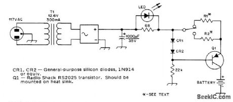
Switch gives choice of two constant-current charge rates. With 10 ohmsfor R1, rate is 60 mA, while 200 ohms for R2 gives 3 mA. Silicon diodes CR1 and CR2 have combined voltage drop of 1.2 V and emitter-base junction of Q1 has 0.6-V drop, for net drop of 0.6 V across R1 or R2. Dividing 0.6 by desired charge rate in amperes gives resistance value.-M. Alterman, A Constant-Current Charger for Nicad Batteries, QST, March 1977, p 49. (View)
View full Circuit Diagram | Comments | Reading(1041)
LED_VOLTAGE_INDICATOR
Published:2009/6/29 21:13:00 Author:May
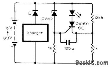
Circuit shown uses LED to indicate, by lighting up, that battery has been charged to desired level of 9 V. Circuit can be modified for other charging voltages. Silicon switching transistor can be used in place of more costlythyristor.-P. R. Chetty, Low Bat-tery Voltage Indication, Wireless World, April 1975, p 175. (View)
View full Circuit Diagram | Comments | Reading(998)
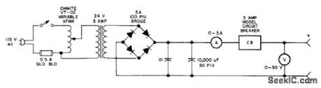
12_V_AT_8_A
Published:2009/6/29 21:08:00 Author:May
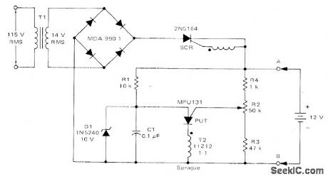
Charging circuit for lead-acid storage batteries is not damaged by short-circuits or by connecting with wrong battery polarity. Battery provides currentfor charging C1 in PUT relaxation oscillator. When PUT is fired by C1, SCR is turned on and applies charging current to battery. Battery voltage increases slightly during charge, increasing peak point voltage of PUT and making C1 charge to slightly higher voltage. When C1 vo!tage reaches that of zener D1, oscillator stops and charging ceases. R2 sets 12 V maximum battery voltage between 10 and 14 V during charge.-R. J. Haver and B. C. Shiner, Theory, Characteristics and Applications of the Programmable Unijunction Transistor, Moto-rola, Phoenix, AZ, 1974,AN-527, p 10. (View)
View full Circuit Diagram | Comments | Reading(2807)
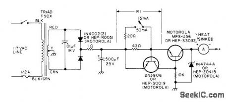
BULK_NICAD_CHARGER
Published:2009/6/29 20:59:00 Author:May
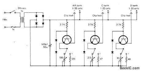
Can handle up to 20 AA cells, 20 C cells, and 20 D cells simultaneouslt, with charging rate determined separately for each type. Single transfrmer and fullwave rectifier feed about 24 VCD to three separate regulators. AA-cell regulator uses 100-ohm resistor to vary charge rate from 6 mA to above 45 mA, C-cell chargerate range is 24 to 125 mA, and D-cell range is 60 to 150 mA. Batteries of each type should be about same state of discharge. Batteries are recharged in series to avoid need for separate regulator with each cell. Tricklecharge switches cut charge rates to about 2% of rated normal charge (5 mA for 500-mAh AA cells).Transistors are 2N4896 or equivalent. Use heatsinks. All diodes are 1N4002.-J.J. Schultz, A Bull Ni-Cad Recharger, CQ, Dec. 1977, p 35-36 and 111. (View)
View full Circuit Diagram | Comments | Reading(775)
High_side_switches_for_33_Voperation
Published:2009/7/24 22:52:00 Author:Jessie
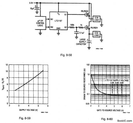
Figure 8-58 shows an LTC1157 connected to provide high-side switching (Chapter 2) for two 3.3-V loads. Figure 8-59 shows the gate-voltage (above supply) characteristics for the LTC1157, which is a dual, low-voltage MOSFET driver specifically designed for operation between 2.7 V and 5.5 V The LTC1157 internal charge pump boosts the gate-drive voltage 5.4 V above the 3.3-V positive supply (or 8.7 V above ground). This voltage fully enhances a logic-level N-channel below 4.6 V, and housekeeping is performed (data storage, etc.) before the batteries are completely discharged. The other three channels of the LTC 1156 act as switches (under microprocessor control) to power the remaining sections of the computer. The number of switches can be increased by adding more LTC1155 or LTC1156 circuits as needed. LINEAR TECHNOLOGY, APPLICATION NOTE 53, P. 11. (View)
View full Circuit Diagram | Comments | Reading(720)
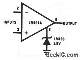
Precision_diode
Published:2009/7/24 22:51:00 Author:Jessie
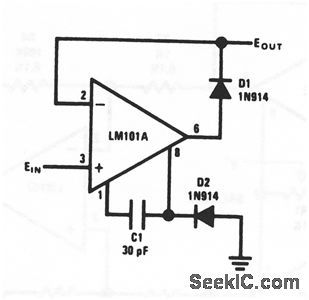
This circuit virtually eliminates diode threshold potential so that millivolt signals can be rectified、Less than 100μV change at the input causes the output of the LM101A to swing from negative to positive. (View)
View full Circuit Diagram | Comments | Reading(756)
CHARGING_SILVER_ZINC_CELLS
Published:2009/6/29 20:52:00 Author:May
Used for initial charging and subsequent rechargings of sealed dry-charged lightweight cells developed for use in missiles, torpedoes, and space applications. Article covers procedure for filling cell with potassium hydroxide electrolyte before placing in use (cells are dry-charged at factory and have shelf life of 5 or more years in that condition). Charge current should be 7 to 10% of rated cell discharge capacity; thus, for Yardney HR-5 cell with rated discharge of 5 A, charge at 350 to 500 mA. Stop charging when cell voltage reaches 2.05V.If used only for battery charging, large filter caacitor can be omitted.-S.Kelly, Will Silver-Zinc Replace the Nicad?, 73 Magazine, Holiday issue 1976, p 204-205. (View)
View full Circuit Diagram | Comments | Reading(624)
12_V_FOR_NICADS
Published:2009/6/29 20:47:00 Author:May
Produces constant current with simple transistor circuit, adjustable to 15 or 50 mA with switch and R1. Zener limits voltage at end of charge. Developed for charging 10-cell pack having nominal 12.5V, as used in many transceivers.-H. Olson, Battery Chargers Exposed, 73 Magazine, Nov.1976, p 98-100 and 102-104. (View)
View full Circuit Diagram | Comments | Reading(794)
Bar_graph_level_gauge
Published:2009/7/24 22:14:00 Author:Jessie
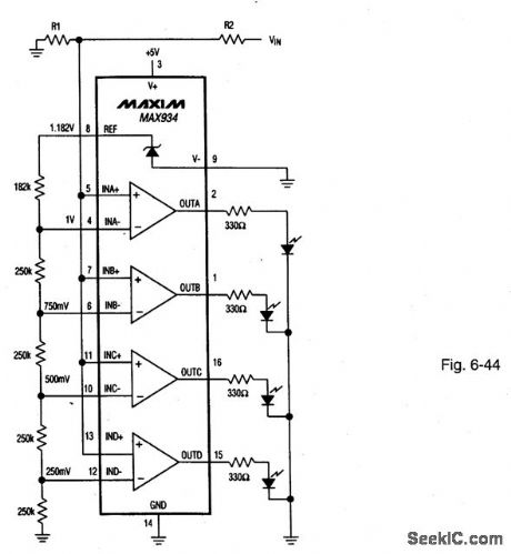
Figure 6-44 shows a MAX934 connected as a simple, four-stage level detector with LED readouts. The full-scale threshold (all LEDs on) is given by VIN=(R1 + R2)/R1 volts. The other thresholds are at 3/4 full-scale, 1/2 full-scale, and 1/4 full-scale. The output resistors limit the current into the LEDs. MAXIM NEW RELEASES DATA BOOK, 1995, P. 3-58. (View)
View full Circuit Diagram | Comments | Reading(1453)
Bilateral_current_source
Published:2009/7/24 22:12:00 Author:Jessie
This circuit is similar to that of Fig. 10-25, except that the adjustment circuit is omitted (and the circuit is simplified). (View)
View full Circuit Diagram | Comments | Reading(0)
Window_detector
Published:2009/7/24 22:11:00 Author:Jessie
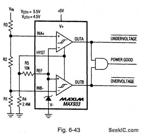
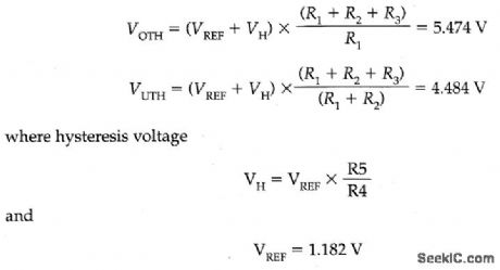
Figure 6-43 shows a MAX933 comparator connected as a window detector (see Fig. 6-42 for pin connections). For the voltage thresholds shown (5.5 V upper and 4.5 V lower), use 249 kΩ, 61.9 kΩ, and 1 MΩ for R1, R2, and R3 respectively. Verify these resistor values using the following equations:Other threshold values can be selected by choice of the R1, R2, and R3, values, using the same equations. MAXIM NEW RELEASES DATA BOOL, 1995, P. 3-57. (View)
View full Circuit Diagram | Comments | Reading(2)
NICKEL_CADMIUM_CELL_CHARGER
Published:2009/6/29 20:43:00 Author:May
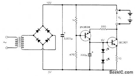
Charges four size D cells in series at constant current, with automatic voltage limiting. BC301 transistor acts as current source, with base voltage stabilized at about 3 V by two LEDs that also serve to indicate charge condition. Other transistor provides voltage limiting when voltage across cekks approaches that of 1k branch of voltage divider. Values shown give 260-mA charge initially, dropping to 200 mA when VC reaches 5V and decreasing almost to 0 when VCreaches 6.5 V.-N.H. Sabah, Battery Charger, Wireless World, Nov. 1975, p 520. (View)
View full Circuit Diagram | Comments | Reading(989)
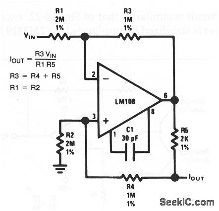
Precision_current_source
Published:2009/7/24 22:43:00 Author:Jessie
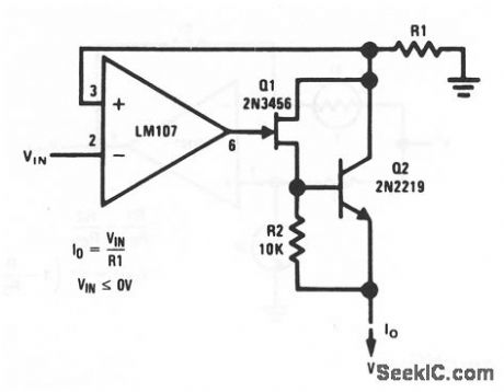
The output of this circuit depends on VIN and the value of R. Notice that VIN can be anything from 0 to (V- +1 V) and V- can be -2 to -35 V. (View)
View full Circuit Diagram | Comments | Reading(0)
33_5_V_from_two_to_three_cells
Published:2009/7/24 23:16:00 Author:Jessie
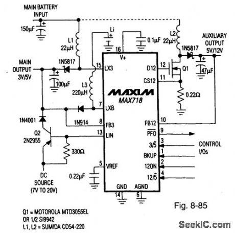
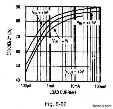
Figure 8-85 shows a MAX718 dual regulator connected to provide a maln 3.3-V/5-V output and an auxiliary 5-V/12-V output, with a 0.9-V to VOUT input range, and a start-up of 1.4 V Quiescent curren(VIN=3 V)is 140 μA for the main 5-V output.and 500 μA with both outputs. The maximum load-current capability of the malnsupply is 400 mA and 120 mA for the auxiliary Supply.Figure 8-86 shows theefficiency curves,The circuit can generate 3.3 V and 5 V, 3.3 V, and 12 V, or 5 V and 12 V, depending on the state of the logic inputs at pms 3 and 4.Two regulatedoutput voltages are generated from one of three input-voltage Sources∶an ac/dc wall-cube adapter(7 V or 20 V), a maln two-cell or three-cell battery,or a backuplithium battery. The dotted-line connection at the top of L2, which Powers theauxiliary supply, is normallv hard-wired to the maln battery,but it can also beconnected to the maln output when Power comes from the ac wall adapter. The main switching regulator automatically shuts off to save the batteries when the ac/dc wall cube is plugged in, MAXIM BATTERY MANAGEMENT CIRCUIT COLLECTION,1994, P.11. (View)
View full Circuit Diagram | Comments | Reading(671)
Dual_35_V_to_5_V_12_V_supply
Published:2009/7/24 23:04:00 Author:Jessie
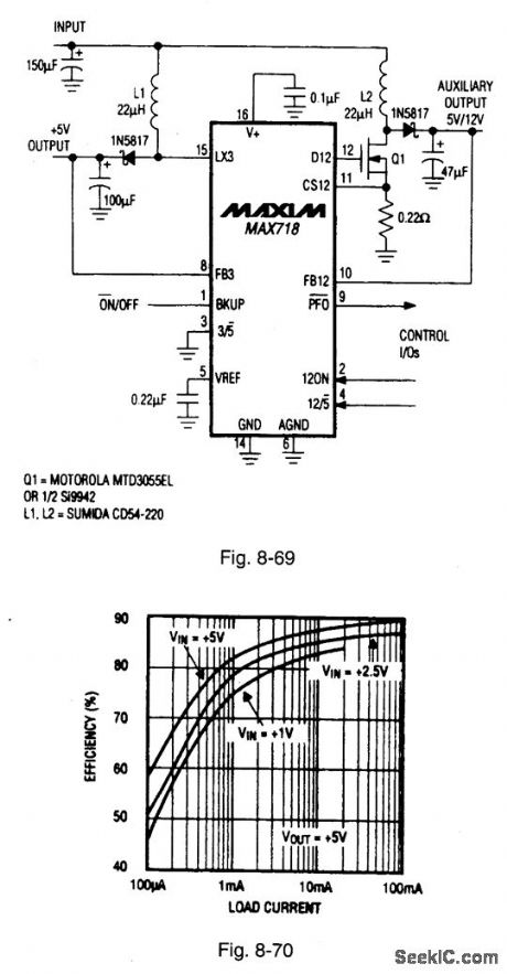
Figure 8-69 shows a MAX718 controller connected to provide 5 V and 12 V from a 3.3-V supply. Figure 8-70 shows the efficiency curves. This circuit is designed for those applications that require a 3.3-V to 5-V converter to supply power for peripheral equipment, and a +12-V supply for flash-memory programming. The circuit delivers 5 V at 400 mA, and 12 V at 120 mA when powered from a 3.3-V (±10%) supply. The 12-V output can be programmed to 5 V, under logic control without external switches or pullup. The input voltage is 0.9 V to VOUT with 1.4-V no-load start-up. Quiescent current is 140 μA for 5 V, and 500 μA for both 5 V and 12 V. The switching frequency is 0.5 MHz. MAXIM BATTERY MANAGEMENT CIRCUIT COLLECTION, 1994, P. 42. (View)
View full Circuit Diagram | Comments | Reading(640)
| Pages:161/291 At 20161162163164165166167168169170171172173174175176177178179180Under 20 |
Circuit Categories
power supply circuit
Amplifier Circuit
Basic Circuit
LED and Light Circuit
Sensor Circuit
Signal Processing
Electrical Equipment Circuit
Control Circuit
Remote Control Circuit
A/D-D/A Converter Circuit
Audio Circuit
Measuring and Test Circuit
Communication Circuit
Computer-Related Circuit
555 Circuit
Automotive Circuit
Repairing Circuit