
Index 179
PRECISION_CURRENT_SOURCE
Published:2009/6/18 23:29:00 Author:May
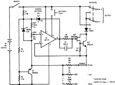
A complete, battery-powered current source suitable for laboratory use is shown. The op amp regulates the voltage acrosg the range resistors at a level determined by the voltage on the arm of the calibrated potentiometer, R3. The voltage on the range resistors is established by the current through Q2 and Q3, which is delivered to the output.The reference diode, D1, determines basic accuracy. Q1 is included to ensure that the LM11 inputs are kept within the common-mode range with diminishing battery voltage. A light-emitting diode, D2, is used to indicate output saturation. However, this indication cannot be relied upon for output-current settings below about 20 nA, unless the value of R6 is increased. The reason is that very low currents can be supplied to the range resistors through R6 without developing enough volt-age drop to turn on the diode.If the LED illuminates with the output open, there is sufficient battery voltage to operate the cir-cuit. But a battery test switch is also provided. It is connected to the base of the op-amp output stage and forces the output toward V+. (View)
View full Circuit Diagram | Comments | Reading(2186)
LOW_LEVEL_SOUNDER
Published:2009/6/18 23:07:00 Author:May
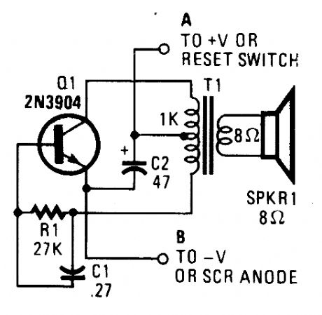
This is a simple low-level noise maker that's ideally suited to certain alarm applications. When the sounder is Iocated in another part of the building, the sound level is loud enough to be heard, but is not loud enough to wam off an intruder. A single 2N3904 npntransistor is connected in a Hartley audio oscillator, with a 1 kΩ to 8-Ω tran-sistor-output transformer doing double duty.The circuit produces a single-frequency tone that can be varied in frequency by changing the value of either or both R1 and C1. Increasing the value of either component will Iower the output frequency and decreasing their values will raise the frequency. Don't go below 4.7 kΩ for R1 because you could easily destroy Q1. (View)
View full Circuit Diagram | Comments | Reading(727)
DUAL_TONE_SOUNDER
Published:2009/6/18 23:04:00 Author:May
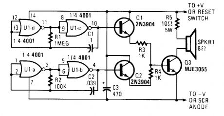
An outside horn-type speaker works best with the circuit. However, such devices require a great deal of power, so this sounder should only be used in alarm circuits where at least a 6-A SCR is used as the sounder driver.A single CMOS 4001 quad 2-input NOR gate, two 2N3904 general-purpose npn transistors, and a single MJE3055 power transistor combine to generate a two-tone output. Gates UI-a and UI-b are configured as a simple feedback oscillator with R2 and C2 setting the oscillator's frequency. With the values shown, the circuit oscillates at about 500 Hz.Gates U1-c and U1-d are connected in a similar oscillator circuit, but they operate at a much lower frequency. The oscillator frequencies (and thus the tones that they produce) can be altered by increasing or decreasing the values of R1 and C1 for the low-frequency oscillator and R2 and C2 for the high-frequency oscillator. Decreasing the values of those components will increase the frequency; increasing their values will decrease the frequency.The two oscillator outputs are connected to separate amplifiers (configured as emitter follow-ers), whose outputs are used to drive a single power transistor (Q3, an MJE3055). A 10-Ω, 5-W re-sistor, R5, is used to limit the current through the speaker and Q3 to a safe level. To boost the sound level, R5 can be replaced with another speaker. (View)
View full Circuit Diagram | Comments | Reading(987)
HIGHLY_STABLE_60_Hz_SINE_WAVE_SOURCE
Published:2009/6/18 21:40:00 Author:May
A highly-stable 60-Hz sine wave can be delivered with this circuit,which offers a different andmuch simpler approach to galnlng a stable amplitude,Capacitor coupling the last stage removes anydc component caused by unequal zener voltages in the clipping circuit that follows the comparator. (View)
View full Circuit Diagram | Comments | Reading(1235)
MULTIPLE_FIXED_CURRENT_SOURCE
Published:2009/6/18 2:21:00 Author:May
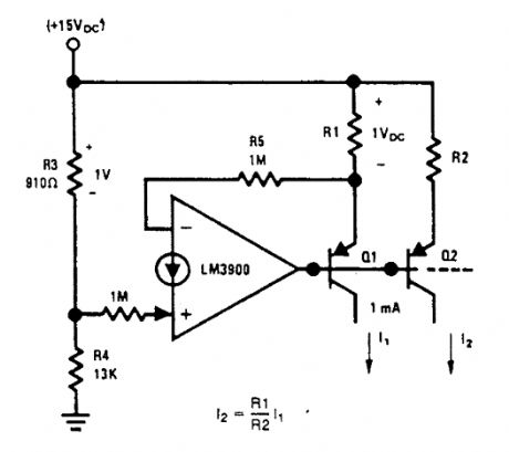


A multiple fixed current source is provided by the circuit. A reference voltage (1 Vdc) is established across resistor R3 by the resistive divider (R3 and R4). Negative feedback is used to cause the voltage drop across RI to also be 1 Vdc.This controls the emitter current of transistor Q1 and if we neglect the small current diverted into the (-) input via the 1-MQ input resistor (13.5μA) and the base current of Q1 and Q2 (an additional 2% loss if the β of these transistors is 100),essentially this same current is available out of the collector of Q1.Larger input resistors can be used to reduce current loss and a Darlington connection can be used to reduce errors caused by the β of Q1.The resistor, R2, can be used to scale the col- lector current of Q2 either above or below the 1-22-4 mA reference value. (View)
View full Circuit Diagram | Comments | Reading(1072)
VOLTAGE_CONTROLLED_CURRENT_SOURCE
Published:2009/6/18 2:12:00 Author:May

A voltage-variable current source is shown in the figure. The transconductance is-(1/R2) as the voltage gain from the input terminal to the emitter of Q1 is-1. For Vin=0Vdc, the output current is essentially 0 mA dc. Resistors R1 and R6 guarantee that the amplifier can turn OFF transistor Q1. (View)
View full Circuit Diagram | Comments | Reading(4529)
12_kW_144_MHz_AMPLIFIER_POWER_SUPPLY
Published:2009/6/18 2:04:00 Author:May
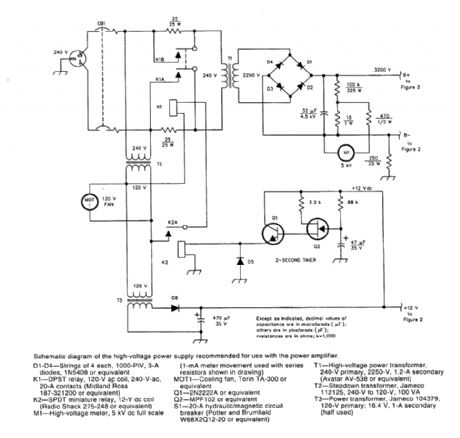
A schematic diagram of the high-voltage power supply recommended for use with the power transformer. This power supply can also be used for other equipment with similar requirements.CAUTION: hazardous high voltages. (View)
View full Circuit Diagram | Comments | Reading(1464)
SIMPLE_POWER_DOWN_CIRCUIT
Published:2009/6/17 3:33:00 Author:May
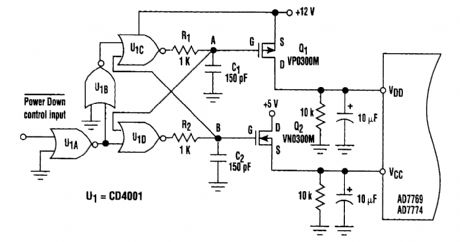
This circuit adds a power-down function to analog I/O ports (for example, the AD7769 and AD7774). Moreover, the diodes ordinarily needed to protect the devices against power-supply mis-sequencing can be eliminated (see the figure).In the circuit, MOSFETs Q1 and Q2 switch the +5- and +12-V supplies, respectively, in a se-quence controlled by two cross-coupled CD4001 CMOS NOR gates (U1C and U1D). The sequence in which power is applied is important: The controlled circuits may be damaged anytimeVCC exceeds VDD + 0.3 V. Consequently, the NOR gates must be powered from a 12-V supply throughout the power-down sequence.Bringing the power down control high (+5 V) applies power to the controlled circuit by turning on all MOSFETs. Specifically, raising the power down brings the output of U1C low, causing capaci-tor C1 to discharge VOL exponentiallywith time constant R1C1. As the voltage on C1 falls, two events occur. First, it puts a negative gate-source voltage on P-channel Q1, turning it on.Second, it causes output gate U1D to go high. With the output of U1D high, capacitor C2 charges exponentially to VOH-about 12-V-applying a positive gate-source voltage to turn on Q2. In the power down mode, the Power Down control is brought low and the RC circuits and their delays work in reverse. Consequently, capacitor C2 discharges to the logic input of U1C before C1 can charge. Hence, Q2 turns off before Q1. (View)
View full Circuit Diagram | Comments | Reading(1036)
SOLID_STATE_LIGHT_SOURCES_11
Published:2009/6/17 3:07:00 Author:May
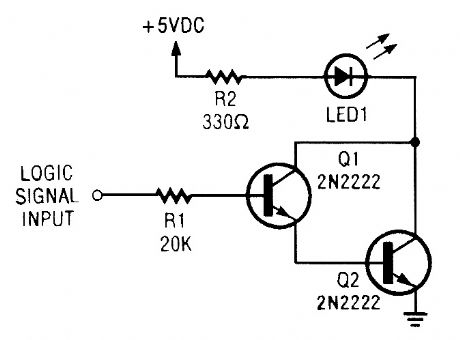
This high sensitivity Darlington LED driver circuit can be used as a simple Iogic probe. You may have to vary the value of R1 to suit the circuit under test. (View)
View full Circuit Diagram | Comments | Reading(821)
SOLID_STATE_LIGHT_SOURCES_10
Published:2009/6/17 3:06:00 Author:May
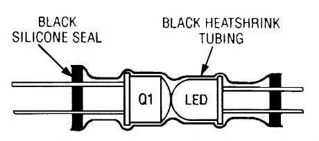
You can “roll your own” optocoupler by using some heat-shrink tubing, an LED, and optical transistor, and silicon sealant as shown here. (View)
View full Circuit Diagram | Comments | Reading(566)
SOLID_STATE_LIGHT_SOURCES_9
Published:2009/6/17 3:06:00 Author:May
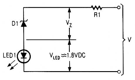
This is a simpler voltage-level sensor than that shown back in Fig. 9, To use it you have to know the polarity of the voltage it is to monitor. (View)
View full Circuit Diagram | Comments | Reading(582)
SOLID_STATE_LIGHT_SOURCES_8
Published:2009/6/17 3:05:00 Author:May
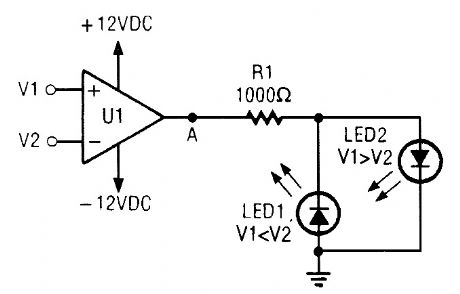
This is a bipolar output indicator that lets you know if one voltage is greater than, less than, or equal to another. (View)
View full Circuit Diagram | Comments | Reading(523)
SOLID_STATE_LIGHT_SOURCES_7
Published:2009/6/17 3:04:00 Author:May
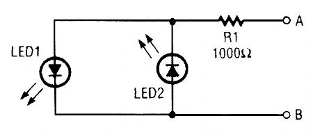
This simple polarity checker is easy to build and can be of help if you don't know much about a circuits wiring or grounding convention (View)
View full Circuit Diagram | Comments | Reading(533)
SOLID_STATE_LIGHT_SOURCES_6
Published:2009/6/17 3:04:00 Author:May
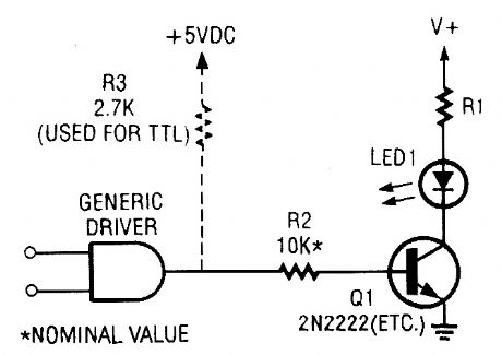
This driver circuit will work for either CMOS or TTL gates, but you don't need R3 in a CMOS-driven circuit. (View)
View full Circuit Diagram | Comments | Reading(557)
SOLID_STATE_LIGHT_SOURCES_5
Published:2009/6/17 3:03:00 Author:May
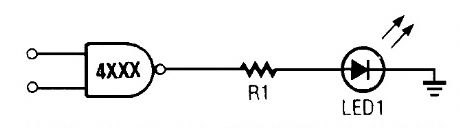
A CMOS-based gate can sink current much like a TTL gate in order to activate an LED. (View)
View full Circuit Diagram | Comments | Reading(591)
SOLID_STATE_LIGHT_SOURCES_4
Published:2009/6/17 3:03:00 Author:May
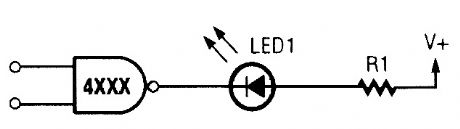
Unlike TTL devices, integrated circuits made with CMOS technology can source enough current to power an LED as shown here. (View)
View full Circuit Diagram | Comments | Reading(566)
SOLID_STATE_LIGHT_SOURCES_3
Published:2009/6/17 3:02:00 Author:May
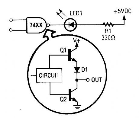
A totem-pole TTL output can drive an LED by grounding the LED's cathode, much like the open-collector driver. (View)
View full Circuit Diagram | Comments | Reading(635)
SOLID_STATE_LIGHT_SOURCES_2
Published:2009/6/17 2:54:00 Author:May
You can drive an LED with an open-collector TTL jnveder. The inveder shown must ground the LED to turn it on. (View)
View full Circuit Diagram | Comments | Reading(607)
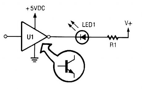
SOLID_STATE_LIGHT_SOURCES_1
Published:2009/6/17 2:54:00 Author:May
Since LED intensity is linearly related to the input current this circuit can be used to vary the LED s brightness via R2 (View)
View full Circuit Diagram | Comments | Reading(602)
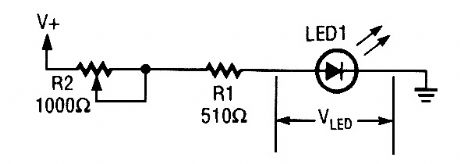
SOLID_STATE_LIGHT_SOURCES
Published:2009/6/17 2:52:00 Author:May

In A we show two LED output curves derived by experiment. The circuit in B was used to get the data for the shod-circuit current plot, while the circuit in C yielded the data for the open-circuit voltage plot. (View)
View full Circuit Diagram | Comments | Reading(557)
| Pages:179/291 At 20161162163164165166167168169170171172173174175176177178179180Under 20 |
Circuit Categories
power supply circuit
Amplifier Circuit
Basic Circuit
LED and Light Circuit
Sensor Circuit
Signal Processing
Electrical Equipment Circuit
Control Circuit
Remote Control Circuit
A/D-D/A Converter Circuit
Audio Circuit
Measuring and Test Circuit
Communication Circuit
Computer-Related Circuit
555 Circuit
Automotive Circuit
Repairing Circuit