
Index 175
TRANSFORMERLESS_dc_POWER_SUPPLY_I
Published:2009/6/23 3:33:00 Author:Jessie
An SCR fires on the positive half cycles of the ac Iine voltage. Switched capacitors are used to select the output voltage. These must all be ac-rated, nonpolarized types. (View)
View full Circuit Diagram | Comments | Reading(778)
SWITCHING_POWER_SUPPLY
Published:2009/6/23 3:31:00 Author:Jessie
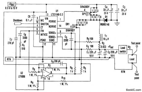
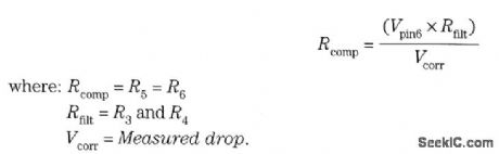
In many switching-regulator applications for portable computers, the microprocessor is located some distance from the power supply. With the latest processors, total load currents range into several amperes. Thus, regulation at the load can become a problem.The ITH pin (pin 6) of the LTC1148 is approximately proportional to the load current. It scales nearly linearly from 0 V at no load to 2.0 V at current limit. U2, acting as a unity-gain differential amplifier, inverts the U1 pin 6 voltage (referenced to SENSE—, pin 7) and causes a current proportional to load current to flow in resistors R5 and R6. A small voltage drop appears across current-sense filter resistors R3 and R4. This' makes the voltage measured by the internal feedback divider appear low. The duty factor is adjusted to bring this back to the correct voltage. As a result, the output is increased slightly as a function of load. Capacitor C9 rolls off the high-frequency gain of the correction amplifier. (View)
View full Circuit Diagram | Comments | Reading(1152)
MASTER_SLAVE_DEVICE_ERROR_CHECKER
Published:2009/6/23 3:30:00 Author:Jessie
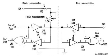
An error-check mechanism introduced into master and slave communication devices can indi-cate mismatches when both the master and slave start sending data simultaneously. The error ftag goes high and indicates a mismatch in the data.The master is the one that can interrupt the communication from a device at the other end and force it to listen. It does this forcing a low voltage level over the communication line by raising the control line to a high level. This inhibits data flow over the tines from the slave device. As a result, the slave turns into a listen mode(not a hardware feature, but rather incorporated in the software). The slave device can transmit the data after communication from the master device ceases. (View)
View full Circuit Diagram | Comments | Reading(1523)
IC_REGULATOR_PROTECTION
Published:2009/6/23 3:55:00 Author:Jessie

This circuit protects an IC regulator against various fault conditions. (View)
View full Circuit Diagram | Comments | Reading(1902)
POWER_SUPPLY_FOR_HIGH_POWER_AUTOSOUND_AMP
Published:2009/6/23 3:53:00 Author:Jessie
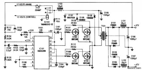
A switching mode inverter is used with a pulse-width modulation voltage regulator (SG35260).Four IRF240 power MOSFETs are used as switches. The output is ±47 V at about 5 A peak. Transformer T101 is a four-turn center tapped primary, and 16-turn center tapped secondary on a Ferrox cube ETD-34 core. (View)
View full Circuit Diagram | Comments | Reading(3826)
FAST_33_V_REGULATOR
Published:2009/6/23 3:45:00 Author:Jessie
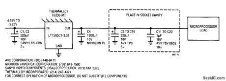


New high-performance microprocessors require a fresh look at power-supply transient response.The LT1585 linear regulator features 1% initial accuracy, excellent temperature drift and load regulation, and virtually perfect line regulation. Complementing superb dc characteristics, the LT1585 exhibits extremely fast response to transients. Transient response is affected by more than the regulator itself. Stray inductances in the layout and bypass capacitors, as well as capacitor ESR dominate the response during the first 400 ns of transient.The ftgure shows a bypassing scheme developed to meet all the requirements for the Intel P44C-VR microprocessor. Input capacitors C1 and C2 function primarily to decouple load transients from the 5-V logic suppJy. The values used here are optimized for a typical 5-V desktop computer silver box powersupply input. C5 to C10 provide bulk capacitance at low ESR and ESL, and C11 to C20 keep the capacitance at low ESR and ESL low at high (>100 kHz) frequencies. C4 is a damper and it minimizes ringing during setting. Trace C is the load current step, which is essentially flat at 4 A with a 20-ns rise time.Trace A is the output settling response at 20 mV per division. Cursor trace B marks -46 mV relative to the initial output voltage. At the onset of load current, the microprocessor socket voltage dips to -38 ntV as a result of inductive effects in the board and capacitors, and the ESR of the capacitors. The inductive effects persist for approximately 400 ns. For the next 3 μs, the output droops as the load current drains the bypass capacitors. The trend then reverses as the LT1585 catches up with the load demand, and the output settles after approximately 50 μs. Running 4 A with a 1.7-V drop, the regulator dissipates 6.8 W. (View)
View full Circuit Diagram | Comments | Reading(1377)
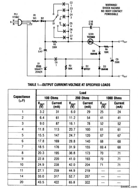
TRANSFORMERLESS_dc_POWER_SUPPLY_II
Published:2009/6/23 3:39:00 Author:Jessie

Although it is simple, this supply can provide 10 to 15 V at 100 mA directly from the ac lines. This circuit has no isolation from the ac line; therefore, there is a shock hazard and it should only be used where no possibility of contacting external devices, circuits, or personnel exists. (View)
View full Circuit Diagram | Comments | Reading(1224)
_5_V_AT_15__TO_3_A_SIPPLY_6__TO__15_V_INPUT
Published:2009/6/23 3:37:00 Author:Jessie
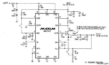
Operating efficiencies of 80 to 90%are possible using the MAX741D and this circuit. (View)
View full Circuit Diagram | Comments | Reading(739)
ROOM_MONITOR
Published:2009/6/23 3:17:00 Author:Jessie
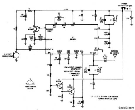
The circuit uses Q1 to buffer the right-channel balance output while Q2 and Q3 form a VOX circuit. When the signal level from the microphone goes high, the output of the VOX also goes high and the multiplexer inside IC1 switches the high-gain left-channel output through to a following buffer stage. This signal is then ac-coupled via C3 into an RE mixer stage and thence to an RF amplifier, which is tuned by C2 and L2. (View)
View full Circuit Diagram | Comments | Reading(3401)
POWER_LINE_MODEM_FOR_COMPUTER_CONTROL
Published:2009/6/23 3:10:00 Author:Jessie
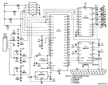
This circuit uses an 87C57 microcontroller and a few peripherals to condition X-10 power-line carrier-code formats from a personal computer to use an X-10 power-line interface in a home-control system. Software details are available in the reference. (View)
View full Circuit Diagram | Comments | Reading(3380)
ac_POWER_LINE_MONITOR
Published:2009/6/23 3:07:00 Author:Jessie
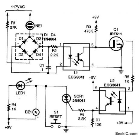
When the power-line voltage source fails,Q1 turns on,activates optoisolator U2, and triggers SCR1.For small SCRs,U1 might directly trigger SCR1. (View)
View full Circuit Diagram | Comments | Reading(1483)
ac_POWER_CONTROLLER
Published:2009/6/23 3:04:00 Author:Jessie
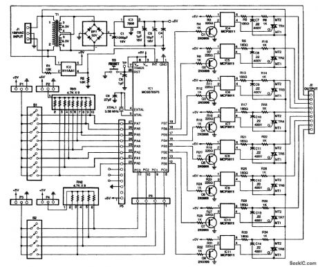
This circuit is used to vary the power delivered to a 120-Vac load under software control. A 68705 micro controller can control eight discrete power triacs, each of which delivers power in 82 smoothly graduated steps, ranging from 0 to 97% of full power. The value delivered to one channel is independent of the value delivered to any other channel. Loads can include light displays, universal motors, heaters, and other appliances.The power level is set by software, not a potentiometer. The software includes a basic set of routines for processing interrupts and setting the power level. The software also includes five test and demonqtration routines for putting the circuit through its paces. Moreover, there's plenty of room to add your own routines to the 68705's built-in EPROM.The basic circuit is simple, yet versatile enough to accept inputs from on-board DIP switches; al-ternatively, the inputs can be driven from a microcomputer bus or parallel port, or a stand-alone device with TTL-compatible outputs. There are 12 input bits to set modes and specify values. (View)
View full Circuit Diagram | Comments | Reading(2134)
NE6O2_dc_POWER_CIRCUITS
Published:2009/6/23 2:38:00 Author:May
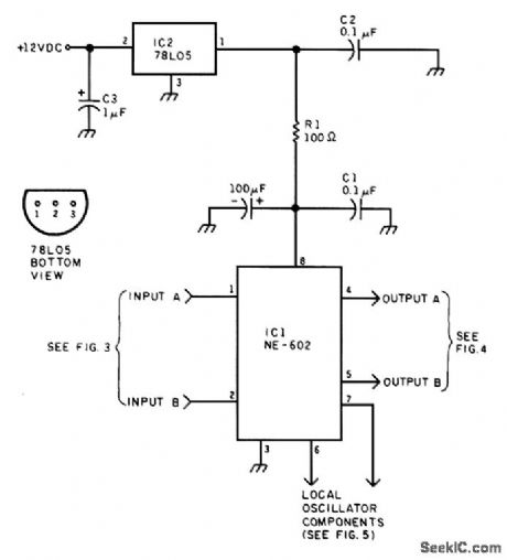
The dc power supply circuit for the NE-602. (View)
View full Circuit Diagram | Comments | Reading(615)
LOOP_OSCILLATOR_ELIMINATOR
Published:2009/6/23 2:50:00 Author:Jessie
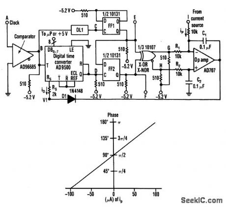
This circuit uses negative feedback to a digital-to-time converter, and can supply a current-con-trolled delay to replace the oscillator in a phase-locked loop that handles input frequencies from 40 kHz to 40 MHz.A current sourced into the inverting input of the op-arrtp integrator's summing node can phase shift the pulses at F in relation to those at E by up to 1800. (View)
View full Circuit Diagram | Comments | Reading(1010)
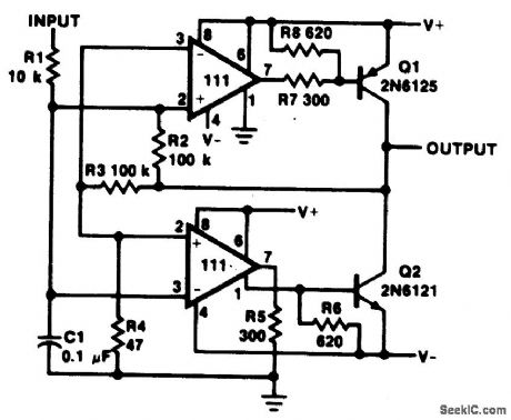
SWITCHING_POWER_AMPLIFIER
Published:2009/6/23 2:14:00 Author:May
View full Circuit Diagram | Comments | Reading(741)
NE602_OUTPUT_CIRCUITS
Published:2009/6/23 2:28:00 Author:Jessie
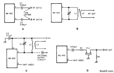
Output circuits for the NE-602. (View)
View full Circuit Diagram | Comments | Reading(676)
NE602_INPUT_CIRCUITS
Published:2009/6/23 2:27:00 Author:Jessie
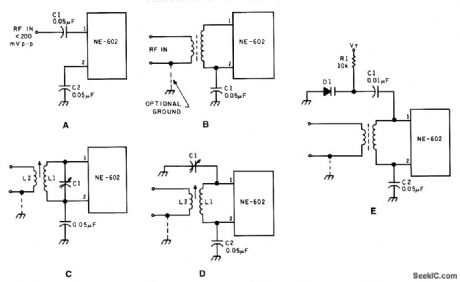
Input circuits for the NE-602. (View)
View full Circuit Diagram | Comments | Reading(1502)
TUNABLE_UHF_OSCILLATOR
Published:2009/6/23 2:27:00 Author:Jessie
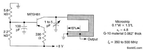
This oscillator is typical for 350- to 500-MHz operation. The microstrip inductor is a PC board trace. The tap is typically 15% from the bottom end. The output power is 55 to 100 mW into 50 Ω, with the frequency stability typically 0.1% over 0 to 50℃. (View)
View full Circuit Diagram | Comments | Reading(2991)
FM_HF_OSCILLATOR_WITH_NO_VARACTOR
Published:2009/6/23 2:25:00 Author:Jessie
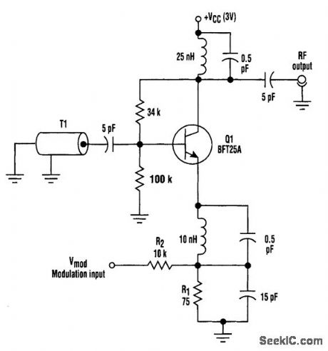
Instead of using a varactor to frequency-modulate a high-frequency oscillator, this circuit uses base-charging capacitance modulation. Consequently, the large voltage change required by a varactor, which can be a major problem in battery-powered systems with limited supply voltages, is elimtnated. T1 is a ceramic coaxial quarter-wave resonator. (View)
View full Circuit Diagram | Comments | Reading(1011)
SIMPLE_PSEUDORANDOM_VOLTAGE_SOURCE
Published:2009/6/23 2:24:00 Author:Jessie
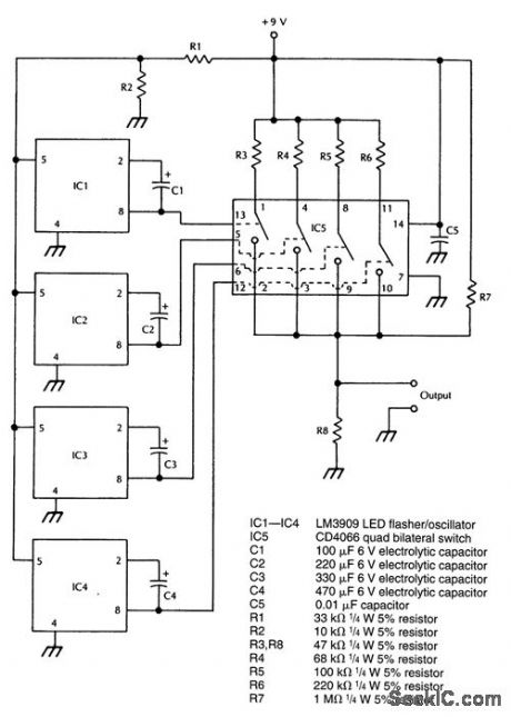
An approximation to a pseudorandom voltage is produced by combining the outputs of four low-frequency oscillators with 0.3, 0.6, 0.9, and 1.4 Hz frequencies. The summing network is a quad bilateral switch and resistor network. (View)
View full Circuit Diagram | Comments | Reading(702)
| Pages:175/291 At 20161162163164165166167168169170171172173174175176177178179180Under 20 |
Circuit Categories
power supply circuit
Amplifier Circuit
Basic Circuit
LED and Light Circuit
Sensor Circuit
Signal Processing
Electrical Equipment Circuit
Control Circuit
Remote Control Circuit
A/D-D/A Converter Circuit
Audio Circuit
Measuring and Test Circuit
Communication Circuit
Computer-Related Circuit
555 Circuit
Automotive Circuit
Repairing Circuit