
Index 174
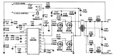
SCR_SWITCHING_SUPPLY_FOR_COLOR_TV_RECEIVERS
Published:2009/6/23 4:09:00 Author:May
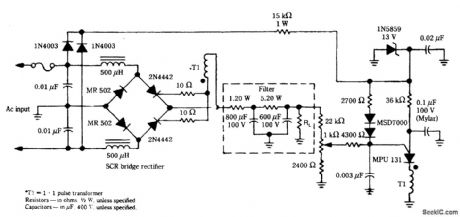
An output +80Vat up to 1.5A is available from this supply. Aminimum load of 200 mA is required because of the SCR hold-ing current. Notice that no ac line isolation is provided and a shock hazard exists. (View)
View full Circuit Diagram | Comments | Reading(688)
POWER_EFFICIENT_VOLTAGE_REGULATOR
Published:2009/6/23 4:06:00 Author:May
Included in the many features of this power-efficient, voltage-regulator circuit is shutdown power control with a current output up to several hundred milliamperes (expandable to amperes, if desired). Current limiting can be preset to a fixed level for controlled dissipation in Q1 and the circuit requires no auxiliary voltage supply for the pass transistor. (View)
View full Circuit Diagram | Comments | Reading(747)
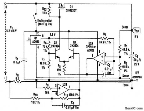
TRACKING_POWER_SUPPLY
Published:2009/6/23 4:03:00 Author:May
Two op amps are used in this basic op-amp regulator circuit. The outputs can be fed to current amplifier stages or emitter followers, if needed. (View)
View full Circuit Diagram | Comments | Reading(966)
SIMPLE_9_V_SUPPLY
Published:2009/6/23 4:02:00 Author:May
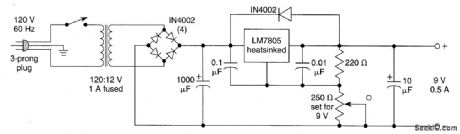
This circuit uses an LM7805 with a resistive voltage divider in the common leg of the regulator.The regulator can be fooled into producing an apparent higher output voltage in this manner. This supply is useful for running radios, tape recorders, or other 9-V devices. (View)
View full Circuit Diagram | Comments | Reading(1150)
5_Vdc_REGULATED_SUPPLY
Published:2009/6/23 4:44:00 Author:Jessie
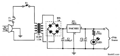
View full Circuit Diagram | Comments | Reading(898)
+5_V_AT_1_A_SUPPLY_WITH+3_TO+5_V_INPUT
Published:2009/6/23 4:43:00 Author:Jessie
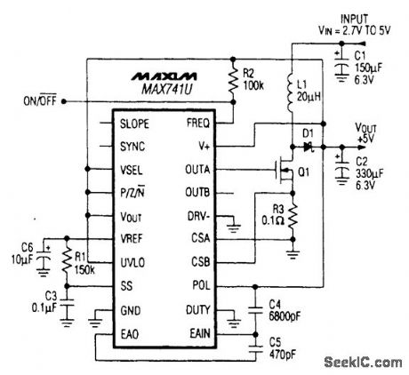
A MAX741U switching-mode power-supply controller and a switching FET Q1 are used to provide +5 V at 1 A. (View)
View full Circuit Diagram | Comments | Reading(697)
SIMPLE_9_V_POWER_SUPPLY
Published:2009/6/23 4:42:00 Author:Jessie
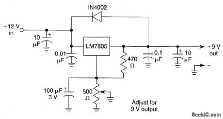
This supply will provide 9-V transistor radios or cassettes from a 12-V auto electrical system. (View)
View full Circuit Diagram | Comments | Reading(767)
MULTIPLE_ON_CARD_REGULATOR_ADJUSTER
Published:2009/6/23 4:41:00 Author:Jessie
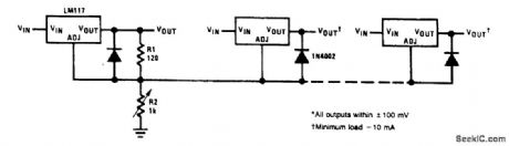
This circuit allows one pot to control several on-card regulators for adjustment within ±100 mV of each other. (View)
View full Circuit Diagram | Comments | Reading(589)
SWITCHED_POWER_CONTROL_CIRCUITS
Published:2009/6/23 4:40:00 Author:Jessie
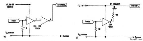
Load currents of a few milliamperes to amperes can be turned on and off by these switched power-control circuits. The U2 CMOS inverter stage works as a simple power switch for load currents less than 5 mA (Fig. 68-27A), allowing easy reference shutdown. If appreciably higher switched output currents are called upon, an alternate CMOS inverter driving a low-threshold PMOS device can be used to switch currents of up to 1 A or more (Fig. 68-27B). (View)
View full Circuit Diagram | Comments | Reading(684)
4_TO_70_V_REGULATOR
Published:2009/6/23 4:39:00 Author:Jessie
This regulator operates from a single supply.If the op amp is not able to control an overvoltage condition, the SCR will crowbar the output. (View)
View full Circuit Diagram | Comments | Reading(693)
12_V_SUPPLY
Published:2009/6/23 4:37:00 Author:Jessie
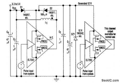
When driving a power MOSFET from a 5-V or 3.3-V system, a significant number of components usually are needed to generate an extra +12 V.It's possible, however, to apply the second channel in a typical dual MOSFET driver to derive a +12-V power supply. By using a driver with the drains brought to separated pins, you can connect an inductor between the n-channel drain and the logic supply without connecting the p-channel device.The driver operates as a standard flyback-style switched-mode circuit (see the figure). When the output n-channel device is on, current starts flowing in the inductor, which stores energy. When the n-channel device is turned off, current must continue flowing. Therefore, it flows through diode D2 to charge up C1 and C2. As the cycle repeats, the C1 and C2 voltage rises until the Zener diode prevents further voltage rise. This is needed to prevent the driver's derived supply from exceeding the part's maximum voltage rating. (View)
View full Circuit Diagram | Comments | Reading(694)
33_V_FROM_5_V_LOGIC_SUPPLIES
Published:2009/6/23 4:36:00 Author:Jessie
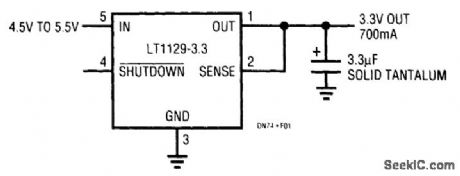
Microprocessor chip sets and logic families that operate from 3.3-V supplies are gaining acceptance in both desktop and portable computers. Computing rates, and in most cases, the energy consumed by these circuits, show a strong improvement over 5-V technology. The main power supply in most systems is still5 V, necessitating a local 5-V to 3.3-V regulator. Linear regulators are viable solutions at lower (IO≤1 A) currents, but they must have a low dropout voltage in order to maintain regulation with a worst-case input of only 4.5 V. The ftgure shows a circuit that converts a 4.5-V minimum input to 3.3Vwith an output tolerance of only 3% (100 mV). The LT1129-3.3 can handle up to 700 mA in surface-mount conftgurations, including both 16-μA shutdown and 50-μA standby currents for system sleep modes. Unlike other Iinear regulators, the LT1129-3.3 combines both low-dropout and Iow-voltage operation. Small input and output capacitors facilitate compact, surface-mount designs. (View)
View full Circuit Diagram | Comments | Reading(600)
SAWTOOTH_GENERATOR
Published:2009/6/23 4:35:00 Author:Jessie
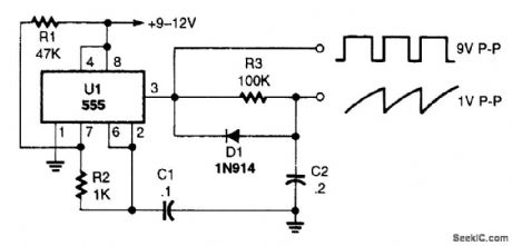
A sawtooth waveform generator circuit using a 555 IC is shown. The IC is connected in an astable oscillator circuit with the majority of the output contained in the positive portion of the cy-cle. The negative output is a very brief pulse.Capacitor C2 charges through R3 in a positive direction during the time that the IC's output (at pin 3) is high. When the output goes negative, C2 is rapidly discharged through Dl and the IC's out-put.Peak-to-peak sawtooth output is about 1 V. The linearity of this circuit is best when R3 is as large as possible. The oscillator's frequency is about 200 Hz and can be increased by lowering either the value of R1 or C1 to decrease the frequency, increase the values of those components. (View)
View full Circuit Diagram | Comments | Reading(5453)
SIMPLE_12_V_POWER_SUPPLY
Published:2009/6/23 4:35:00 Author:Jessie
This 12-V power supply is easy-to-build,and it produces a smooth output,D1 is a 14-V,1/2-W Zener diode. The voltage can be varied by a few volts up or down to change the output voltage (View)
View full Circuit Diagram | Comments | Reading(805)
OP_AMP_LINEAR_SAWTOOTH_GENERATOR
Published:2009/6/23 4:34:00 Author:Jessie
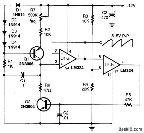
Q1 is connected in a simple constant-current generator circuit. The value of Q1's emitter resistor sets the constant-current level flowing from the transistor's collector to the charging capacitor, C1.One op amp of an LM324.quad op-amp IC, UI-a, is connected in a voltage-follower circuit. The input impedance on the voltage follower is very high and offers little or no load on the charging cir-cuit. The follower's output is connected to the input of UI-b, which is configured as a voltage com-parator. The comparator's other input is tied to a voltage-divider setting the input level to about 8 V.The output of UI-b at pin 7 switches high when the voltage at its positive input, pin 5, goes above 8 V. That turns on Q2, discharging C1. The sawtooth cycle is repeated over and over as long as power is applied to the circuit.The sawtooth's frequency is determined by the value of C1 and the charging current supplied to that capacitor. As the charging current increases, the frequency also increases, andvice versa, To in-crease the generator's frequency range, decrease the value of C1, and to lower the frequency, in-crease the value of C1. The output is about 3 to5V. (View)
View full Circuit Diagram | Comments | Reading(3806)
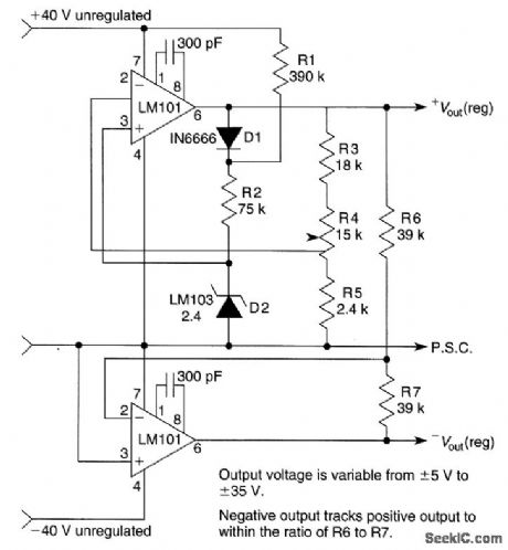
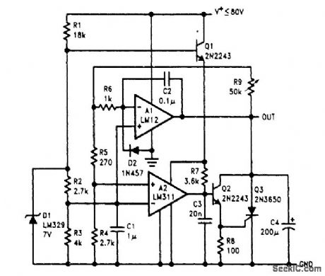
POSITIVE_REGULATO_WITH_o_TO_70_V_OUTPUT
Published:2009/6/23 4:34:00 Author:Jessie
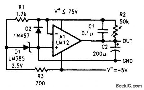
The op amp has one input at ground and a reference current drawn from its summing junction. With this arrangement, the output voltage is proportional to setting resistor R2. A negative supply is used to operate the op amp within its common-mode range, providing zero output with sink current and power a low-voltage bandgap reference, D1. The current drawn from this supply is under 150 mA, except when sinking a load current. The output load capacitor, C2, is part of the op-amp frequency compensation. (View)
View full Circuit Diagram | Comments | Reading(1300)
LOW_NOISE_5_V_SUPPLY
Published:2009/6/23 4:23:00 Author:Jessie
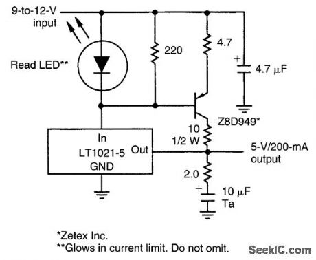
Standard three-terrrtinal regulator ICs can be noisy. The key is the noise over the 10-Hz to 10-kHz band; measurements revealed a 40-dB improvement over standard three-terminal regulators.The regulator is built around a 5-V buried-Zener reference. It's the buried Zener's inherently low noise that makes the finished supply so quiet. Measured over a 10-Hz to 10-kHz band, the 5-V out-put contains just 7 μV rms of noise at full load. The 10-Hz to 10-kHz noise can be further reduced to 2.5 μV rms by adding a 100-p,H, 1000-μF output filter. The noise characteristics of the reference are tested and guaranteed to a maximum of 11 μV over the band of interest.An extemal boost transistor, the ZBD949, provides gain to meet a 200-mA output current requirement. Current limiting is achieved by ballasting the pass transistor and clamping the base drive.Although the oscillator only requires 200 mA, it's possible to extend the output current to at least 1 A. (View)
View full Circuit Diagram | Comments | Reading(908)
NE6O2_POWER_SUPPLY_OPTIONS
Published:2009/6/23 4:00:00 Author:Jessie
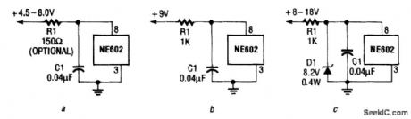
Here, Figs. 68-11A through 68-11C show an RC-filter used as both current limiter (R1) and integrator (C1), as well as for isolation. In Fig. 68-11A, +4.5 to 8.0 Vdc is the normal operating range of the NE602. In Fig. 68-11B, R1 drops voltage, and is used because a +9-V battery can go higher, and a +9-Vwall supply can produce up to 11 V. In Fig. 68-11C, a +8- to 18-Vdc supply is regulated using a 8.2-V Zener for D1. (View)
View full Circuit Diagram | Comments | Reading(543)
33_V_SWITCHING_REGULATOR
Published:2009/6/23 3:59:00 Author:Jessie
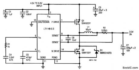


For the LT1129-3.3, dissipation amounts to a little under 1.5 W at full output current. The 5-lead surface-mount DD package handles this without the aid of a heatsink, provided that the device is mounted over at least 2500 mm2 of ground or power-supply plane. Efficiency is around 62%; dissi-pation in linear regulators becomes prohibitive at higher current levels, where they are supplanted by high-efficiency switching regulators. The synchronous buck converter is implemented with an LTC1148-3.3 converter. The LTC1148 uses both Burst ModeTM operation and continuous, constant off-time control to regulate the output voltage, and maintain high efficiency across a wide range of output loading conditions. (View)
View full Circuit Diagram | Comments | Reading(2065)
1IC_REGULATOR_PROTECTION
Published:2009/6/23 3:56:00 Author:Jessie
This circuit protects an IC regulator against various fault conditions. (View)
View full Circuit Diagram | Comments | Reading(1951)
| Pages:174/291 At 20161162163164165166167168169170171172173174175176177178179180Under 20 |
Circuit Categories
power supply circuit
Amplifier Circuit
Basic Circuit
LED and Light Circuit
Sensor Circuit
Signal Processing
Electrical Equipment Circuit
Control Circuit
Remote Control Circuit
A/D-D/A Converter Circuit
Audio Circuit
Measuring and Test Circuit
Communication Circuit
Computer-Related Circuit
555 Circuit
Automotive Circuit
Repairing Circuit