
Index 165
Step_down_voltage_regulator
Published:2009/7/25 3:03:00 Author:Jessie
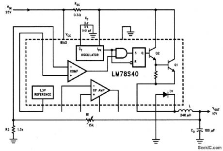
This circuit converts 25-V to an adjustable 10-V output at 500 mA, with less than 1% ripple. (View)
View full Circuit Diagram | Comments | Reading(1403)
Step_up_voltage_regulator_with_increased_voltage_current_ratings
Published:2009/7/25 2:46:00 Author:Jessie
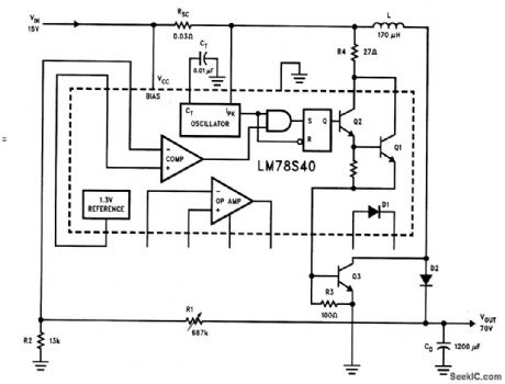
This circuit is similar to that of Fig. 4-65, except that the input is 15 V, and the output is 70 V with less than 1% ripple. (View)
View full Circuit Diagram | Comments | Reading(1089)
Step_up_voltage_regulator
Published:2009/7/25 2:45:00 Author:Jessie
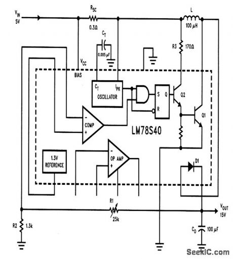
This circuit converts 5-V to an adjustable 15-V output at 150 mA, with less than 1 % ripple. (View)
View full Circuit Diagram | Comments | Reading(802)
Off_line_regulator_with_a_floating_intput
Published:2009/7/25 2:44:00 Author:Jessie
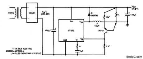
With this circuit, the input of the LT1070 switching regulator floats to a potential set by the output. (View)
View full Circuit Diagram | Comments | Reading(757)
Negative_to_positive_switched_capacitor_converter
Published:2009/7/25 2:43:00 Author:Jessie
This circuit is similar to that of Fig. 4-56, except that the input is negative and the output is positive. (View)
View full Circuit Diagram | Comments | Reading(711)
Switched_capacitor_12_to_5_V_converter
Published:2009/7/25 2:42:00 Author:Jessie
This circuit provides 5 V at 1 A from a 12-V input. (View)
View full Circuit Diagram | Comments | Reading(599)
The op-amp μA741 switch power supply circuit
Published:2011/7/24 3:53:00 Author:Seven | Keyword: op-amp, switch power supply
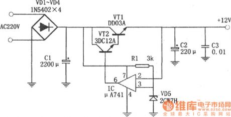
The power supply adopts with the op-amp μA741 as the comparator control element, 2 triodes as the regulating elements, the circuit is working the the open state. When the output voltage is 2mV lower than the Vref, i.e the 2-pin is 2mV lower than 3-pin(as the sensibility ofμA741 is 2mV), 6-pin of μA741 is outputting a high LEV, VT1 and VT2 are conducting, large current load and relevant capacitors of C2 and C3 compensate the power, soon the output voltage rises to 12V, i.e 2-pin and 3-pin of μA741 have the same LEV.
(View)
View full Circuit Diagram | Comments | Reading(1182)
Switched_capnacitor_5__to_±10_V_converter
Published:2009/7/25 2:41:00 Author:Jessie
This circuit uses charge-pump principles to convert 5 V to ±10 V at 10 mA. At no load, the output is ± 13 V. (View)
View full Circuit Diagram | Comments | Reading(731)
Switched_capacitor_6__to_±7_V
Published:2009/7/25 2:40:00 Author:Jessie
This circuit provides±7-V outputs at 20 mA from a 6-V input. (View)
View full Circuit Diagram | Comments | Reading(504)
Switched_capacitor_5_V_to±12_V_converter
Published:2009/7/25 2:39:00 Author:Jessie
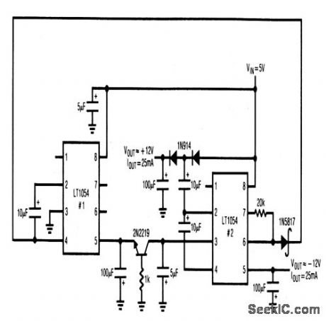
This circuit provides ±12-V outputs at 25 mA from a 5-V input. (View)
View full Circuit Diagram | Comments | Reading(584)
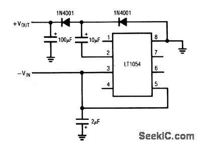
Switched_capacitor_voltage_boost_converter
Published:2009/7/25 2:38:00 Author:Jessie
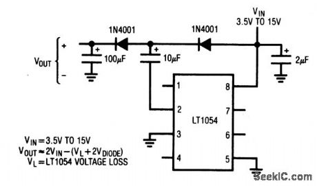
This circuit boosts the input voltage (to almost double),using two diodes and the LT1054. (View)
View full Circuit Diagram | Comments | Reading(892)
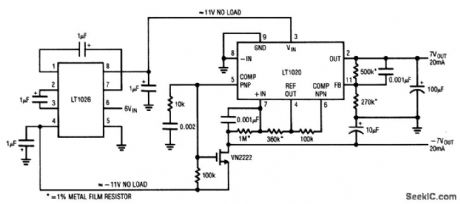
Switched_capacitor_6__to_±5_V_converter_
Published:2009/7/25 2:37:00 Author:Jessie
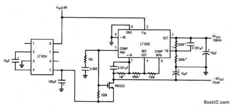
This circuit provides a +5-V output at 100mA and -5-V output at 75mA from a 6-V input. (View)
View full Circuit Diagram | Comments | Reading(595)
Basic_switched_capacitor_converter_
Published:2009/7/25 2:36:00 Author:Jessie
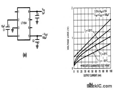
This circuit shows how a switched-capacitor building-block LT1054 can be used to convert positive input voltage to negative output voltage, with losses as shown in Fig.4-56B. (View)
View full Circuit Diagram | Comments | Reading(782)
15__to_10_V_Converter_with_20000_V_isolation
Published:2009/7/25 2:35:00 Author:Jessie
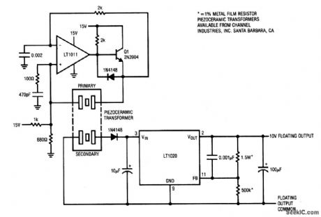
This circuit uses a piezoceramic transformer to isolate the output from the inputs. Common-mode voltages of 20,000 V are acceptable. (View)
View full Circuit Diagram | Comments | Reading(670)
Isolated_15__to_1000_V_converter
Published:2009/7/25 2:33:00 Author:Jessie
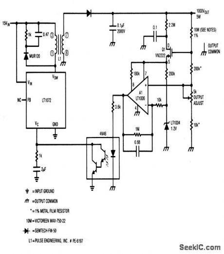
This circuit provides the same function as that of Fig. 4-53, except that the output is isolated (floating). Common-mode voltages of 2000 V are accept-able. (View)
View full Circuit Diagram | Comments | Reading(676)
Nonisolated_15__to_1000_V_converter
Published:2009/7/25 2:32:00 Author:Jessie
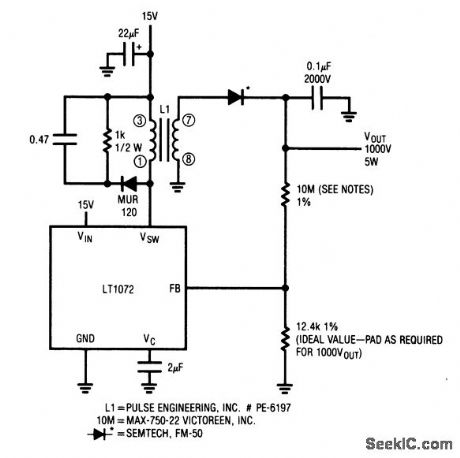
This circuit is suitable for use with photomultiplier tubes, ion generators, gas-based detectors, image intensifiers, or any application where the supply does not need to be isolated from the load. (View)
View full Circuit Diagram | Comments | Reading(682)
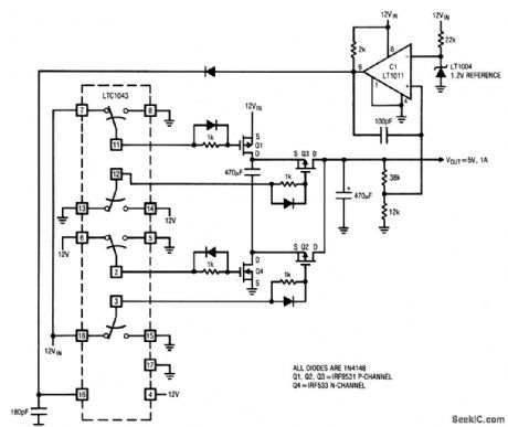
Linear_regulator_with_switching_pre_regulator
Published:2009/7/25 2:30:00 Author:Jessie
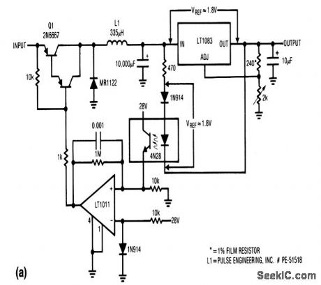
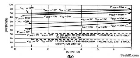
This circuit provides linear regulation (chapter 7), but with switching pre-regulation. The combination permits good efficiency with a wide range of input and output voltages, as shown in Fig. 4-52B (efficiency versus output current). (View)
View full Circuit Diagram | Comments | Reading(2065)
Positive_buck_boost_converter
Published:2009/7/25 2:28:00 Author:Jessie
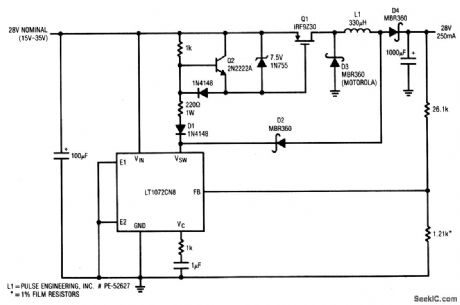
This circuit provides 28-V output at 250 mA for inputs from 15 to 35 V. (View)
View full Circuit Diagram | Comments | Reading(1158)
Positive_buck_converter_with_wide_input_range
Published:2009/7/25 2:25:00 Author:Jessie
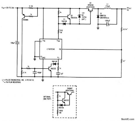
This circuit provides 5-V output at 5 A, for inputs from 12 to 35 V. If the PMOS transistor is replaced with a Darlington pnp transistor (shown in dashed lines), efficiency decreases. (View)
View full Circuit Diagram | Comments | Reading(941)
Positive_to_negative_flyback_converter_with_wide_mput_range
Published:2009/7/25 2:22:00 Author:Jessie
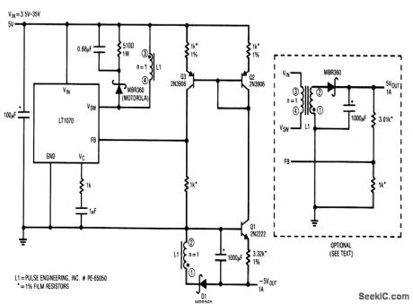
his circuit provides -5-V output at 1 A, for inputs from +3.5 to +35 V. Q1 introduces a -2 mV/℃ drift. This drtft can be compensated by the circuit showrn in dashed lines,although line regulation is somewhat degraded. (View)
View full Circuit Diagram | Comments | Reading(712)
| Pages:165/291 At 20161162163164165166167168169170171172173174175176177178179180Under 20 |
Circuit Categories
power supply circuit
Amplifier Circuit
Basic Circuit
LED and Light Circuit
Sensor Circuit
Signal Processing
Electrical Equipment Circuit
Control Circuit
Remote Control Circuit
A/D-D/A Converter Circuit
Audio Circuit
Measuring and Test Circuit
Communication Circuit
Computer-Related Circuit
555 Circuit
Automotive Circuit
Repairing Circuit