
Index 178
BATTERY_STATUS_INDICATOR
Published:2009/6/22 22:29:00 Author:May
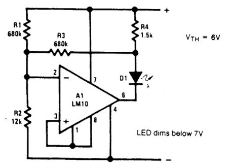
In battery-powered circuitry, there are some advantages to having an indicator to show when the battery voltage is high enough for proper circuit operation. This is especially true for instruments that can produce erroneous data.The battery status indicator is designed for a 9-V source. It begins dimming noticeably below7V artd it extinguishes at 6 V. If the warning of incipient battery failure is not desired, R3 can be re-rnoved and the value ofJR, is halved. (View)
View full Circuit Diagram | Comments | Reading(3)
LOW_BATTERY_CIRCUIT
Published:2009/6/22 22:25:00 Author:May
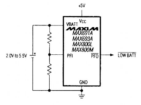
A Maxim MAX691A series IC allows low-battery detection. (View)
View full Circuit Diagram | Comments | Reading(960)
BATTERY_CHARGER_PROBE
Published:2009/6/22 22:25:00 Author:May
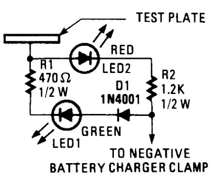
This battery-charger probe can keep you from damaging batteries or yourself by testing to see if the charger is already on and/or connected improperly.To use the probe, the positive cable clamp is first connected to the positive battery terminal. Then, the test plate is touched to the negative terminal of the battery. If the battery is connected properly, current will pass from the test plate through RI, LED1, Dl, the negative charger, and into the positive side of the batteries. If LED1 (the green LED) lights, you can clamp on the negative lead and turn on the charger.If the terminals are reversed, current will flow in the opposite direction, causing LED2 to light, warning you of danger. When the cable is reversed, Dl protects LED1 from excessive reverse volt-age. If that happens, immediately turn the power off, and right the cable connections. Finally, if the battery charger is on, both LEDs will light because chargers actually produce pulsating dc and rely on the battery to act as a filter. (View)
View full Circuit Diagram | Comments | Reading(873)
BATTERY_BUTLER
Published:2009/6/22 22:17:00 Author:May
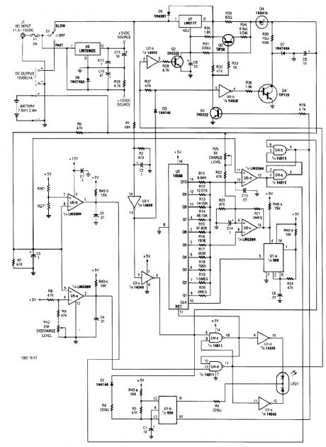
The battery butler solves the common problems associated with the maintenance and operationof NiCad batteries The battery butler,by initially discharging a NiCad battery to a preset point,reduces the possibility of the“memory”effect occurring,Once discharged,a battery is then usuallycharged at 25%and reduce the internal cell pressure increase by 40% or more Once the battery ISfully charged,a trickle charge IS provided to maintain the battery In a fully charged state The battery butler circuit can be bypassed,and the existing fast-charger used,if needed (View)
View full Circuit Diagram | Comments | Reading(1683)
NICAD_BATTERY_CHARGER_1
Published:2009/6/19 3:13:00 Author:May
This circuit has a current regulator and uses an external timer to control the charging rate. (View)
View full Circuit Diagram | Comments | Reading(1180)
2_TO_5_CELL_LITHIUM_BATTERY_CHARGER
Published:2009/6/19 3:06:00 Author:May
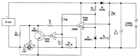
A more generally applicable circuit-design concept for recharging lithium batteries could easily accommodate different cell types and various numbers of cells. That's because both the charger out-put-voltage set point and current limit, or maximum charging current, can be adjusted by simply changing a resistor. (View)
View full Circuit Diagram | Comments | Reading(1018)
NICAD_CHARGER_ZAPPER
Published:2009/6/19 3:04:00 Author:May
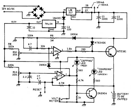
This NiCad charger/zapper has a built-in charger and zapper circuit to clear shorted NiCads. This circuit delivers a high-current pulse to trim out internal shorts. (View)
View full Circuit Diagram | Comments | Reading(1718)
NICAD_BATTERY_CHARGER
Published:2009/6/19 2:53:00 Author:May
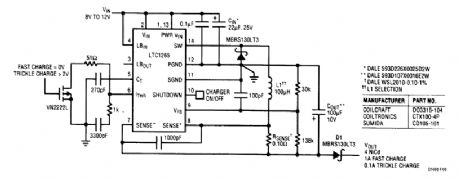
The LTC1265 is configured as a battery charger for a four-NiCad stack. It has the capability of performing a fast charge of 1A, a trickle charge of 100mA, or the charger can be shut off. In shut-off, diode D1 serves two purposes. First, it prevents the LTC1265 circuitry from drawing battery current and second, it elintinates back powering the LTC1265, which avoids a potential latch condition at powerup. (View)
View full Circuit Diagram | Comments | Reading(1977)
THREE_CELL_LITHIUM_CHARGER
Published:2009/6/19 2:52:00 Author:May
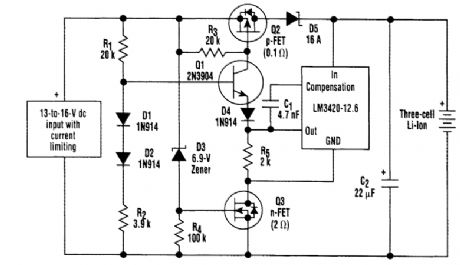
This 3-A, three-cell charging circuit for lithium batteries includes a built-in on/off switch made up of Q3, R4, and D3. When a dc input is present, D3 turns on Q3, which allows current to flow through the LM3411 and Q1. If dc voltage is removed, Q3 turns off, cutting battery drain to zero. (View)
View full Circuit Diagram | Comments | Reading(997)
SINGLE_CELL_LITHIUM_BATTERY_CHARGER
Published:2009/6/19 2:50:00 Author:May
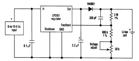
An LP2951 regulator was chosen for this single lithium cell-charging circuit for its built-in cur-rent-limiting capability. In addition, the regulator's output voltage is extremely stable, which is a pre-requisite for lithium battery charging. This figure details an example circuit designed to recharge a single cell. The required output set voltage was specified as 4.200 V (±0.025 V) with a maximum charging current of about 150 mA.An LP2951 regulator was selected for two reasons. One is that its built-in current limiter holds the maximum current to 160 mA (typical). The other is because the output voltage can be very ac-curately set to 4.200 V, thanks to the regulator's stable internal bandgap reference.The 1.23-V reference appears between the feedback pin and ground, which causes a precise current to flow in the output resistive-divider string. The amount of current flowing in these resis-tors determines (sets) the charger output voltage that appears across the battery terminals. Large-value resistors keep the battery drain below 2μA when the dc input is removed (a customer requirement). A trimming potentiometer sets the output to 4.200 V. It must be adjusted when the battery isn't connected to the charger output. A blocking diode is required at the LP295l's output to prevent current from flowing out of the battery and back into the output when the dc-input source is removed. Because the diode is in series with the output, the minimum input-output voltage dif-ferential required for this circuit to operate is about 1.5 V. (View)
View full Circuit Diagram | Comments | Reading(1553)
SMART_BATTEY_CHARGER
Published:2009/6/19 2:45:00 Author:May
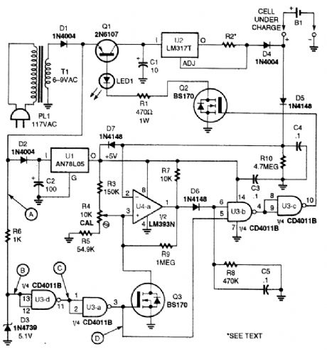
This charger will work with NiCad or the new rechargeable alkaline batteries. The Smartcharger is comprised mainly of four chips-an AN78L05 5-V, 100-mA regulator (U1), an LM317T 1-A adjustable-voltage regulator (U2), a CD4011BE quad 2-input NAND gate (U3), and an LN393N dualvoltage comparator (U4). The value and rating of R2 is selected as described irt the text. R2 is selected for a l.2-V drop across it at the charging current (3Ω for 400 mA, 6Ω for 200 mA). (View)
View full Circuit Diagram | Comments | Reading(2327)
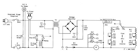
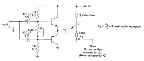
CAR_AUDIO_POWER_SUPPLY
Published:2009/6/19 2:35:00 Author:May
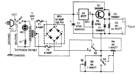
This supply has a variable output voltage feature and a dual voltage switch, S2. Q1 should be ad-equately heatsinked. (View)
View full Circuit Diagram | Comments | Reading(642)
The main circuit block diagram of single phase conversion type UPS power supply
Published:2011/4/11 1:12:00 Author:may | Keyword: single phase conversion type, UPS power supply
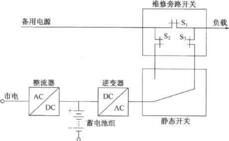
The main circuit block diagram of setting static switch single phase conversion type UPS power supply
UPS power supply can be divided into conversion type and parallel operation type according to compound mode of inverter. The main circuit block diagram of setting static switch single phase conversion type UPS power supply is shown in the diagram. From the diagram we can know that: when it’s in commercial power and normal work, adopt inverter as main power supply and energy supply to load. In order to let maintenance easy, it set a manual maintenance bypass switch, namely when maintaining, first let bypass switch S close, then let S2, S3 and static switch cut. The system changing to use back up supply to energy supply to load, then UPS system and bypass system separate, at this time can maintain to inverter, static switch. When adopting inverter as main power supply, first close static switch and bypass switch S2, S3, then cut S1. (View)
View full Circuit Diagram | Comments | Reading(2354)
AC 110V-DC 12V/8A switching power supply
Published:2011/4/23 3:59:00 Author:May | Keyword: AC 110V-DC 12V/8A, switching power supply
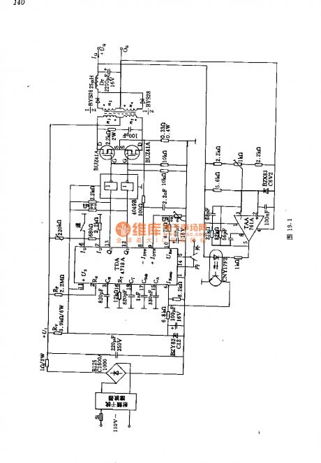
In this circuit, it generates about 150V DC voltage after the AC voltage passing bridge rectifying and capacitor filtering. It is chopped by two power MOS transistor BUZ41A with 50kHz. Then it changes to 18V AC voltage by transistor. Finally, it is full wave rectifying and filtering to output 12V DC voltage. Integrated circuit TDA4718 in the circuit can generate 100kHz high frequency oscillation. It can limit the voltage drop on total power supply resistor by utilizing its current limiting circuit. The output of integrated circuit TDA4718 can drive power transistor by CMOS six-inverter 4049.
Transformer data: n1=n2=67 turns, 30×0.1mm copper lacquered wire (double) ;
n3=n4=9 turns, 2×60×0.1mm copper lacquered wire (double) .
Choke data: 10 turns, 4×30×0.1mm copper lacquered wire. (View)
View full Circuit Diagram | Comments | Reading(3118)
BASIC_COMPLEMENTARY_CLASS_AB_POWER_AMPLIFIER
Published:2009/6/19 1:41:00 Author:May
View full Circuit Diagram | Comments | Reading(711)
THREE_TERMINAL_REGULATOR_CURRENT_SOURCE
Published:2009/6/18 23:56:00 Author:May
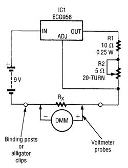
A three-terminal voltage regulator acts as a current source in this circuit. A resistor is being calibrated using a DMM and the current source. (View)
View full Circuit Diagram | Comments | Reading(778)
BASIC_COMPLEMENTARY_CLASS_AB_SINGLE_SUPPLY_AMPLIFIER
Published:2009/6/18 23:56:00 Author:May
View full Circuit Diagram | Comments | Reading(639)
POWER_SUPPLY_FOR_10_MHz_FREQUENCY_STANDARD
Published:2009/6/18 23:55:00 Author:May
This simple power supply can be used in place of battery B1 of the 10-MHz frequency standard. (View)
View full Circuit Diagram | Comments | Reading(646)
0V to 12V adjustable regulated voltage circuit
Published:2011/3/30 2:13:00 Author:muriel | Keyword: 0V to 12V, adjustable, regulated voltage
View full Circuit Diagram | Comments | Reading(573)
0.6-1.5V/2-6A regulated voltage circuit
Published:2011/5/5 3:03:00 Author:muriel | Keyword: 0.6-1.5V/2-6A, regulated voltage circuit
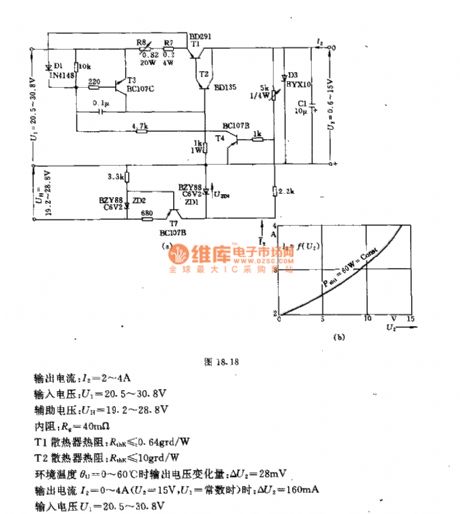
When it uses the auxiliary power supply Uh, Itcanregulate output voltage low to U2 = 0.6 V(FIG. A). After Adjusted the potentiometer R8, itcan changethe load current of limitation whichmakes transistor loss powerless than its maximum allowable (FIG. B). The circuit of the main technical data:Technology data of the circuit: output voltage:U2=0.6V~15V output current:I2=2A~4A input voltage:U1=20.5V~30.8V internal resistance:Rg=40mΩ T1Radiator thermal resistance:Rthk≤0.64grd/W T2Radiator thermal resistance:Rthk≤10grd/W when ambient temperatureθu=0°C~60°C output voltage variable quantity: ΔU2=28mV when output current I2=0~4A(U1=constant,U2=15V), ΔU2=160mV input voltage U1=20.5~30.8V (View)
View full Circuit Diagram | Comments | Reading(587)
| Pages:178/291 At 20161162163164165166167168169170171172173174175176177178179180Under 20 |
Circuit Categories
power supply circuit
Amplifier Circuit
Basic Circuit
LED and Light Circuit
Sensor Circuit
Signal Processing
Electrical Equipment Circuit
Control Circuit
Remote Control Circuit
A/D-D/A Converter Circuit
Audio Circuit
Measuring and Test Circuit
Communication Circuit
Computer-Related Circuit
555 Circuit
Automotive Circuit
Repairing Circuit