
Index 142
FONT_face=VerdanaRSUB1_SUB_RSUB2_SUB_–_VSUB1_SUB_VSUB2_SUB_FONT_frequency_converter
Published:2009/7/23 23:44:00 Author:Jessie
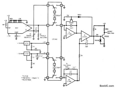
Fig, 12-16 This circuit produces an output frequency that is proportional to the ratio of voltages across two external resistors. The circuit has wide application in transducer signal-conditioning (chapter 14). Both R1 and R2 are ground-referred for noise considerations. In this particular circuit, R1 is a platinum resistance sensor and R2 is set at the R1 0℃ value. The circuit may be used with any resistive-based transducer. For negative TC devices, reverse the positions of R1 and R2. The grounded end of R2 allows fine trimming with decade boxes (if necessary to compensate for R1 tolerances at 0°) without excessive noise problems. The grounded side of R1 permits RI to be located at the end of a cable run (again without noise problems). The DAC serves as a simple source of two identical currents (The DAC MSB is set high, with all other bits low). With constant and equal currents, R1 and R2 produce a differential voltage, which is sampled by the LTC1043 switched-capacitor in the normal manner. To trim, place R1 in a 100℃ environment and adjust the full-scale trim for a 1-kHz output. Linear Technology. Linear Applications Handbook, 1990 p. AN14-17. (View)
View full Circuit Diagram | Comments | Reading(801)
15_A_negative_adjustable_voltage_regulator
Published:2009/7/23 23:44:00 Author:Jessie
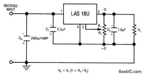
The LAS18U is a four-terminal adjustable regulator IC with an output range from -2.6 to -30 V, adjustable from a single pot. Characteristics are shown in Fig. 7-42B, 7-42C, and 7-42D. (View)
View full Circuit Diagram | Comments | Reading(756)
Wideband_FET_input_composite_buffer_
Published:2009/7/23 23:44:00 Author:Jessie
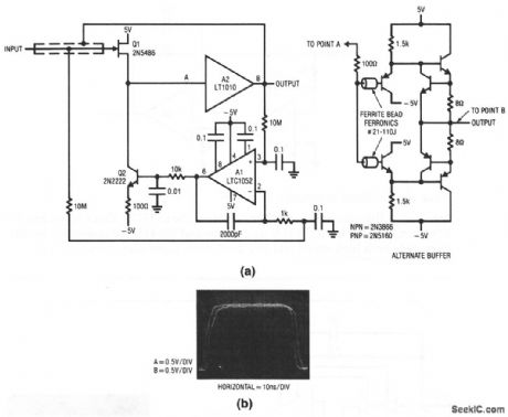
This composite circuit provides a gain of 0.95 with a full power bandwidth near 50 MHz and a slew rate of 2000 V/μs. Offset is about 5μV. Figure 1-19B shows a delay between input and output of about 4 ns. (View)
View full Circuit Diagram | Comments | Reading(695)
15_A_negative_fixed_voltage_regulator
Published:2009/7/23 23:43:00 Author:Jessie
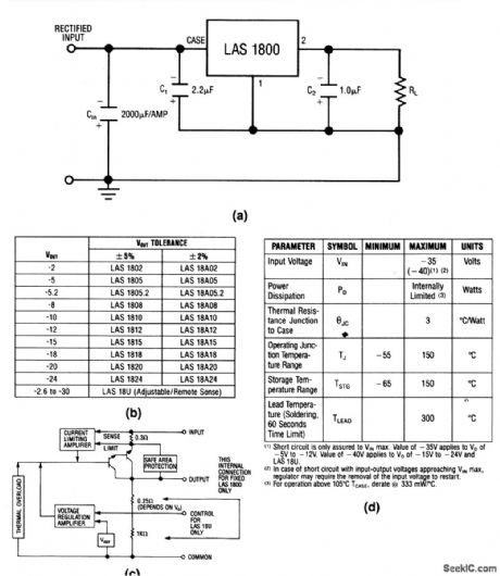
The LAS1800 series voltage regulators are ICs that contain all elements necessary for linear regulation (safe-area protection, thermal overload, current limiting, as shown in Fig. 7-42C). Figure 7-42B shows the output voltage and tolerance for the various LAS1800 part numbers. Figure 7-42D shows the absolute maximum ratings. (View)
View full Circuit Diagram | Comments | Reading(757)
ESUBX_SUB_transfer_function_V_F_converter
Published:2009/7/23 23:43:00 Author:Jessie
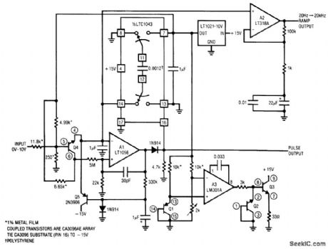
Fig. 12-15 This circuit responds exponentially to the input voltage and is ideally suited for electronic music synthesizers. The circuit has a 1-V-in/octave-offrequency-out scale factor, with exponential conformity with 0.13% over a 10-Hz to 20-kHz range, and 150 ppm/℃ drift. Both a pulse output and a ramp output are available (the ramp is used where substantial power at the fundamental frequency is required). To trim, ground the Q3 base and adjust the 2-kΩ potentiometer so that the A3 inverting input is 100 mV above the noninverting input. Remove the ground at Q3. Linear Technotogy Linear Applications Handbook 1990, p AN14-15. (View)
View full Circuit Diagram | Comments | Reading(656)
Step_down_PWM_switch_mode_regulators
Published:2009/7/23 23:43:00 Author:Jessie
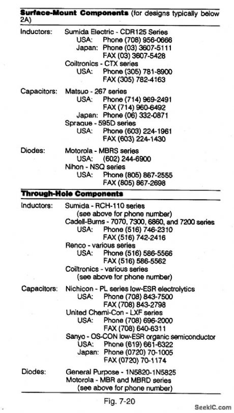
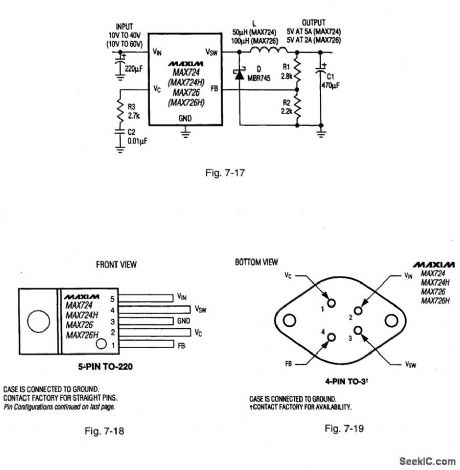
Figure 7-17 shows the MAX724/26 connected as basic step-down converters,Figures 7-18 and 7-19 show the pin configurations.Figure 7-20 shows component suppliers.MAXIM EVALUATION KIT DATA Book, 1994, P. 3-131, 3-131, 3-139. (View)
View full Circuit Diagram | Comments | Reading(724)
8_A_positive_fixed_voltage_regulator_with_remote_sensing
Published:2009/7/23 23:56:00 Author:Jessie
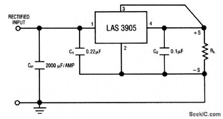
This circuit uses the LAS3905 IC (Fig.7-50) as a voltage regulator with remote sensing. Characteristics are shown in Fig.7-50B, 7-50C, and 7-50D. (View)
View full Circuit Diagram | Comments | Reading(850)
D_C_VOLTAGE_COMPARATOR
Published:2009/7/24 Author:Jessie
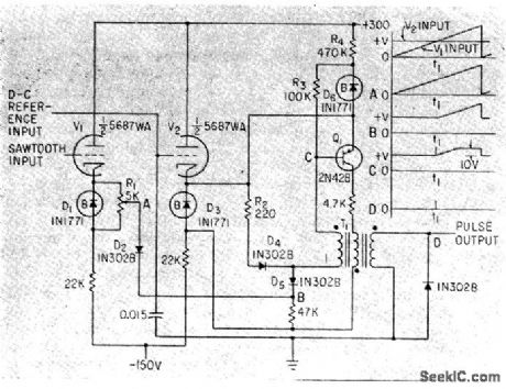
Compares long-duration sawtooth input with d-c reference and generates pulse when inputs coincide.-R. D. Valentine, D-C Voltage Comparator Circuit Uses Tube and Transistor, Electronics, 34:24, p 66. (View)
View full Circuit Diagram | Comments | Reading(726)
Negative_output_F_V_converter
Published:2009/7/24 Author:Jessie
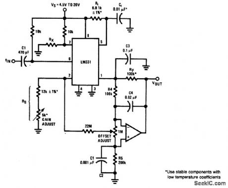
Fig. 12-24 This circuit is similar to that of Fig. 12-19, but with an output/buffer op amp connected to provide a negative output voltage. The 1-MΩ offset adjust can be set to accommodate variations in supply voltage (with 0-V output for a grounded or 0-Hz input). Because the offset voltage is taken from the stable 1.9-V reference voltage from pin 2 of the LM331, any supply-voltage shifts cause no output shifts. Although 1-MΩ is shown, the offset potentiometer can have any value between 200 kΩ and 2 MΩ. The optional bypass capacitor C2 (across R5) prevents output noise arising from stray noise pickup at the noninverting input of the op amp. To trim, set the 5-kΩ gain-adjust control for -10-V output with a 10-kHz input. National Semiconductor Linear Applications Handbook 1991 p 1302. (View)
View full Circuit Diagram | Comments | Reading(743)
_5_V_to_±12_V_±15_V_converter_module
Published:2009/7/23 23:59:00 Author:Jessie
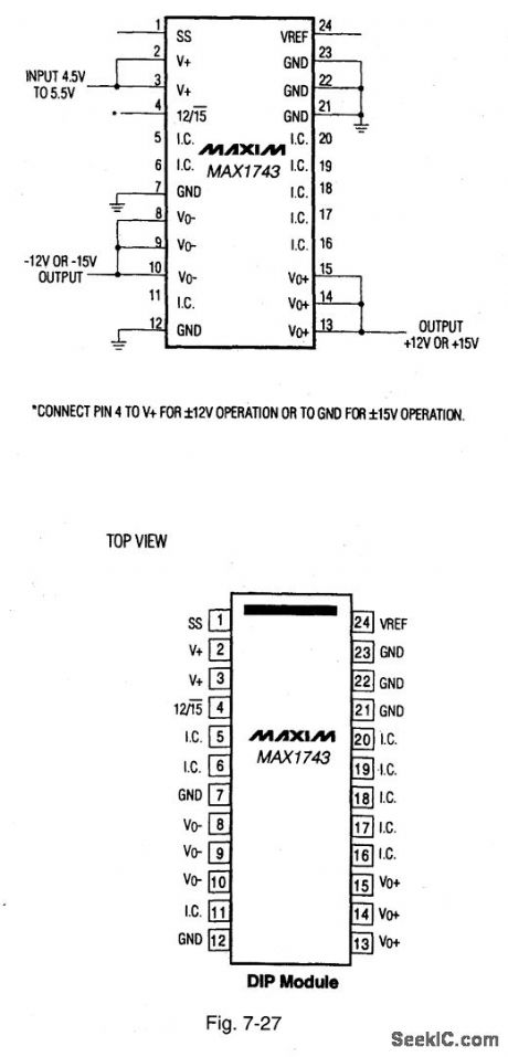
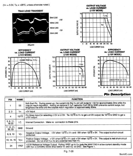
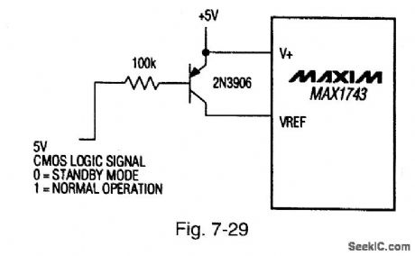
Figure 7-27 shows a MAX1743 3-W converter module that requires no external components. The module supplies 125 mA at 112 V or 100 mA at 115 V. Pin strapping selects 112-V or 115-V operation. Figure 7-28 shows the pin descriptions and operating characteristics. Figure 7-29 shows an optional stand-by mode circuit. MAXIM NEW RELEASES DATA Book, 1994, P. 4-27, 4-29, 4-30.
(View)
View full Circuit Diagram | Comments | Reading(632)
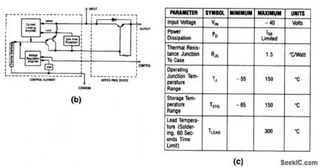
5_A_negative_adjustable_voltage_regulator_with_safe_area_protection
Published:2009/7/23 23:59:00 Author:Jessie
This circuit uses the basic LAS79HG IC and external components to provide safe-operating-area protection. Characteristics are shown in Fig. 7-56B and 7-56C. (View)
View full Circuit Diagram | Comments | Reading(649)
Basic_F_V_converter_with_temperature_compensation
Published:2009/7/23 23:58:00 Author:Jessie
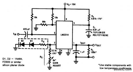
Pig. 12-23 This circuit is similar to that of Fig. 12-19, but with temperature compensation. RX, D1, and D2 cancel the effect of timing capacitance TC. The manufacturer recommends that the circuit be checked with an oven if TC is critical. Resistance can be added in parallel or series with RX to offset the timing capacitor TC If TC is not critical, use 240 kΩ for RX. Again, set the 5-kΩ gain adjust for 10-V output with a 10-kHz input. National Semiconductor Linear Applications Handbook 1991 p 1301. (View)
View full Circuit Diagram | Comments | Reading(616)
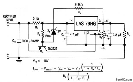
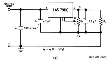
5_A_negative_adjustable_voltage_regulator_with_remote_sensing_and_current_limiting_at_6_A
Published:2009/7/23 23:58:00 Author:Jessie
This circuit uses the basic LAS79HG IC and external components to provide both remote sensing and current limiting. Characteristics are shown in Fig. 7-56B and 7-56C. (View)
View full Circuit Diagram | Comments | Reading(673)
HIGH_VOLTAGE_SUPPLY
Published:2009/7/3 2:44:00 Author:May
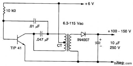
Circuit NotesA 6 V battery can provide 100-150 Vdc center-tapped at a high internal impedance (not dangerous though it can inflict an unpleasant jolt). A 6.3 V transformer is connected in reverse with a transistor used in a Hartley oscillator configuration. The frequency of operation may be controlled by varying the value of the 10 K ohm resistor. The 10 μF capacitor must have a working voltage of at least 250 Vdc. (View)
View full Circuit Diagram | Comments | Reading(0)
HIGH_VOLTAGE_GEIGER_COUNTER_SUPPL
Published:2009/7/3 2:39:00 Author:May
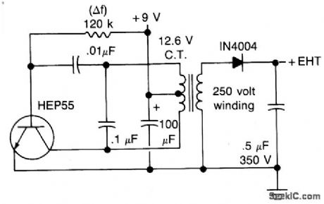
Circuit NotesThis circuit will generate about 300 volts dc-at a very low current,but enough for a GMtube. (View)
View full Circuit Diagram | Comments | Reading(1169)
SIMPLE_HIGH_VOLTAGE_SUPPLY
Published:2009/7/3 2:37:00 Author:May
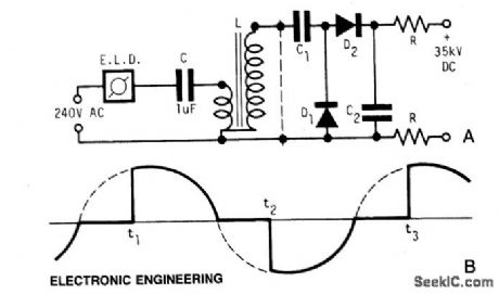
Circuit NotesA light dimmer, a 1 pF capacitor and a 12 V car ignition coil form the simple line powered HV generator. The current in the dimmer is shown in Fig. B. At times t1, t2,..., set by the dimmer switch, the inner triac of the dimmer switches on, and a very high and very fast current pulse charges the capacitor through the primary of the induction coil. Then at a rate of 120 times per second for a 60 Hz line, a very high voltage pulse appears at the secondary of the coil. To obtain an HV dc output, use a voltage doubler. D1 and D2 are selenium rectifiers (TV 18 Siemens or ITT) used for the supply of television sets. High value output shock protection resistors, R, are recommended when suitable. (View)
View full Circuit Diagram | Comments | Reading(2712)
VACUUM_TUBE_AUDIO_AMPLIFIER_POWER_SUPPLY
Published:2009/7/24 4:04:00 Author:Jessie
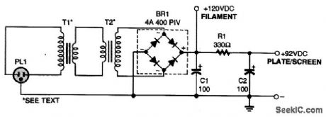
A suitable power supply that provides isolation from the 120-Vac line is shown. The circuit uses two filament transformers connected back to back. The secondary voltages can be almost any value, as long as they are equal. A 1:1 isolation transformer can be substituted, if available. The transformers should be rated at least 25 VA or more. (View)
View full Circuit Diagram | Comments | Reading(802)
15_A_positive_adjustable_voltage_regulator_1
Published:2009/7/24 0:03:00 Author:Jessie


The LLM is a three-terminal adjustable regulator IC with an output range from +1.2 to +37V, with the output voltage set by two external resistors. Because the regulator is floating, higher output voltages can be obtained as long as the maximum input-output voltage differential is not exceeded. Characteristics are shown in Fig. 7-59B, 7-59C, and 7-59D. (View)
View full Circuit Diagram | Comments | Reading(984)
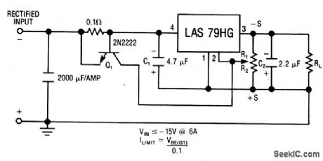
5_A_negative_adjustable_voltage_regulator
Published:2009/7/23 23:57:00 Author:Jessie
The LAS79HG is four-terminal adjustable-regulator IC with an output range from -2.6 to 30 V, providing remote sensing from a single pot. Characteristics are shown in Fig. 7-56B and 7-56C. (View)
View full Circuit Diagram | Comments | Reading(868)
Basic_F_V_converter_with_cascade_transistor
Published:2009/7/23 23:57:00 Author:Jessie
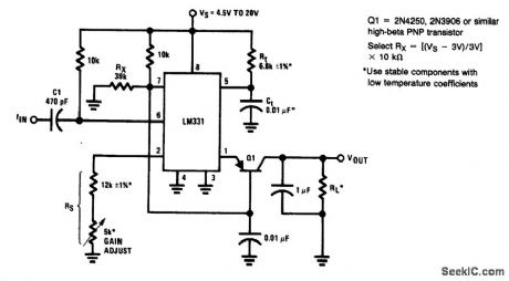
Fig. 12-22 This circuit is similar to that of Fig. 12-19, but with a cascade transistor at the output to improve nonlinearity to 0.006% (typical). Again, set the 5-kΩ gain adjust for 10-V output with a 10-kHz input. National Semiconductor, Linear Applications Handbook 1991 p 1299. (View)
View full Circuit Diagram | Comments | Reading(822)
| Pages:142/291 At 20141142143144145146147148149150151152153154155156157158159160Under 20 |
Circuit Categories
power supply circuit
Amplifier Circuit
Basic Circuit
LED and Light Circuit
Sensor Circuit
Signal Processing
Electrical Equipment Circuit
Control Circuit
Remote Control Circuit
A/D-D/A Converter Circuit
Audio Circuit
Measuring and Test Circuit
Communication Circuit
Computer-Related Circuit
555 Circuit
Automotive Circuit
Repairing Circuit