
Index 177
The +5V solid output step-down convert power supply circuit composed of MAX639
Published:2011/7/24 2:13:00 Author:Seven | Keyword: step-down, power supply
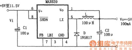
In the figure is the +5V solid output step-down convert power supply circuit composed of MAX639. MAX639 is a high-power step-down DC/AC converter. The input voltage ranges from 5.5V to 11.5V, the output is the +5V solid voltage or the adjustable voltage, the output current is 100mA, the converting efficiency is higher than 90%. The circuit has the function of low battery voltage detection and working/disable mode control.
(View)
View full Circuit Diagram | Comments | Reading(742)
The 20W switch DC voltage stabilizing power supply circuit
Published:2011/7/24 2:05:00 Author:Seven | Keyword: DC voltage, power supply
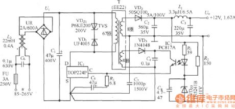
The technique indicators of the power supply are shown as follows:AC input voltage range: u=85~265V; input grid frequency: fLl=47~440Hz; Output voltage (Io=1.67A): Uo=12V;MAX output power: IOM=1.67A; Continuous output power: Po=20W(TA=25℃ or 15W(TA=50℃);Voltage adjusting ratio: η=78%; Output wave voltage MAX value: ±60mV; Working temperature range: TA=0~50℃.
(View)
View full Circuit Diagram | Comments | Reading(991)
VOCAL_STRIPPER_POWER_SUPPLY
Published:2009/6/22 23:33:00 Author:May
The power supply schematic for the lead vocal filter circuit. (View)
View full Circuit Diagram | Comments | Reading(680)
The damming switch power supply circuit
Published:2011/7/21 3:42:00 Author:Seven | Keyword: damming switch, power supply circuit
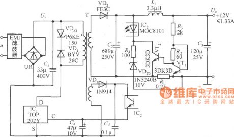
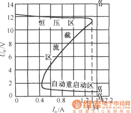
The circuit adopts with a TOP202Y integrated circuit. The damming control loop consists of VTl, VT2, Rl~R4 and IC2. VT1 and VT2 have the consistent parameters, which compose the mirror image current source. The output features of the damming switch power supply is shown in the figure, the output curve can be divided into 3 areas: the constant voltage area, the damming area and the auto restart area. In the figure is the damming switch power supply circuit and curve. (View)
View full Circuit Diagram | Comments | Reading(732)
WWV_CONVERTER
Published:2009/6/22 23:37:00 Author:Jessie
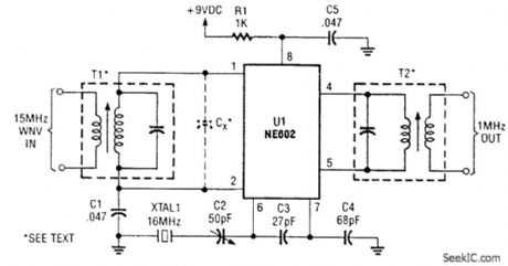
This converter heterodynes the 15-MHz WWW signal with a 16-MHz oscillator so that it can be heard at 1 MHz on an ANI broadcast receiver. T1 and T2 are a modified 10.7-MHz IF transformer and AM BO oscillator coil, respectively. (View)
View full Circuit Diagram | Comments | Reading(2434)
+12_V_FLASH_MEMORY_PROGRAMMING_SUPPLY
Published:2009/6/22 23:07:00 Author:May
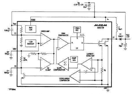
The MAX734 can deliver up to 120 mA @12 V from a +5-V supply, using few external compo-nents. This supply can also be used for other applications than memory programming. A logic level is used for shutdown. Efficiency is about 85%. (View)
View full Circuit Diagram | Comments | Reading(836)
COMPUTER_POWERED_RS_232
Published:2009/6/22 23:05:00 Author:May
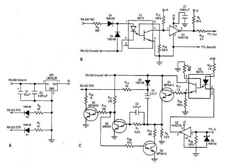
Commercializing battery-operated equipment that must interface to a computer via the RS-232 port runs into the problem of power consumption. To load the system batteries strictly to power the interface is unacceptable. An alternative is to let the computer that the device is connected to pro-vide the interface's power. One snag is that the RS-232 specification doesn't have a power tap on the connector, but it does provide RTS and DTR (request to send and data terminal ready) signals that assert a negative voltage in their quiescent state.Figure 18-GA shows a simple scheme of deriving a 5-V potential from the RTS and DTR signals.R7 and R8 and diodes Dl and D2 mix the return current to the RS-232 port so that the RTS and DTR drivers split the current drawn by the interface. This scheme, even from a laptop computer, can sup-ply 12 rnA to the interface. The only drawback is that the TTL device must be isolated from the cora-puter's ground (earth ground) because the interface treats the RS-232 ground as a positive voltage.A modified optocoupler system shifts the RS-232 level to TTL voltages (Fig. 18-6B). It will sup-port up to 9600 bits/s. C3 is charged up to about 1 V less than the RTS voltage while the TTL line as-serts a marking state. As the capacitor is charging, Q3 is biased into saturation, thus providing a negative voltage (with respect to RS-232 ground) to the RS-232 RXD line. When a spacing bit is driven from the TTL line, Q3 switches off and Q4 switches on. This biases Q4's emitter up to the RS-232 ground. That ground potential is summed with C3's charge to create an RS-232-compatible spacing signal (approximately 1 V less than a -VRTS)The discharge rate on C3 is limited by R15 to prevent the signal sag from becoming a problem down to 110 bits/s. The C2/R1 time constant must be fairly close (within 4 times) to the C3/R15 time constant to ensure that Q3 turns off correctly. (View)
View full Circuit Diagram | Comments | Reading(780)
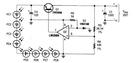
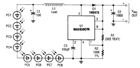
RECHARGEABLE_SOLAR_POWER_FOR_SUN_TRACKER
Published:2009/6/22 23:01:00 Author:May
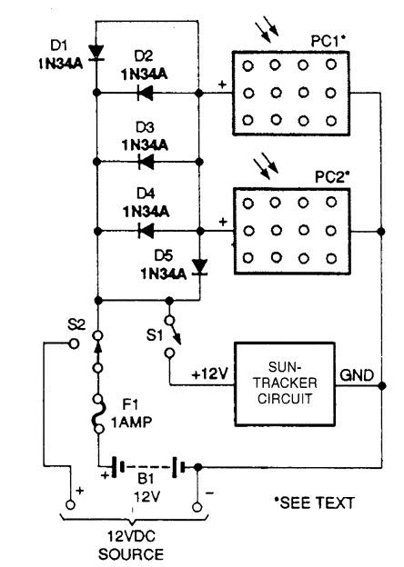
This application circuit provides rechargeable solar power for the sun tracker, as well as for another 12-volt device. PC1 and PC2 can be mounted on sun tracker assembly. (View)
View full Circuit Diagram | Comments | Reading(1704)
PRACTICAL_DIFFERENTIATOR
Published:2009/6/22 23:18:00 Author:Jessie
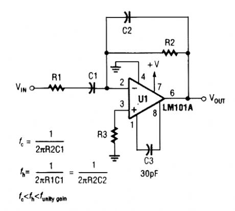
A differentiator has a high-pass charactenstic. Components are chosen by using the design equations. (View)
View full Circuit Diagram | Comments | Reading(1475)
The 3-terminal voltage stabilizer circuit
Published:2011/7/24 7:49:00 Author:Seven | Keyword: 3-terminal, voltage stabilizer
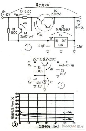
In the figure, resistor R1 provides bias current for the 3-terminal voltage stabilizer, and the need of R1<Veb2/Ib(max) must be met, if R1 is too high, the need in the above formula can't be met, the 3-terminal bias current is provided by base electricity of triode Tr2, and the output voltage is out of control.In figure 1, the output current of 0~5V is almost provided by Tr2, the power of Tr2 is large, so a radiator is needed.
A regulator diode can also form a simple regulator circuit, but the output current is only 10mA or so. (View)
View full Circuit Diagram | Comments | Reading(736)
CAPACITANCE_MULTIPLIER
Published:2009/6/22 23:17:00 Author:Jessie
View full Circuit Diagram | Comments | Reading(0)
PHASE_LOCKED_LOOP
Published:2009/6/22 23:15:00 Author:Jessie
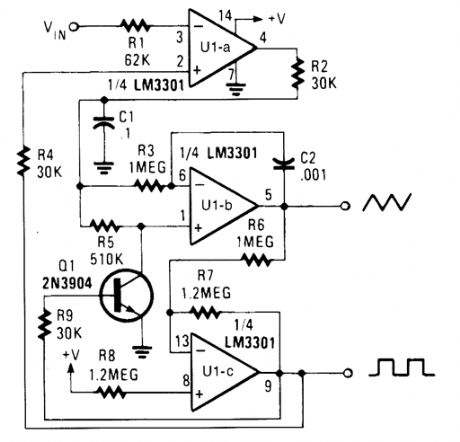
The PLL will lock onto an input signal. Both triangle- and square-wave outputs are available.A quad op amp can be used in this circuit, which should be useful in the audio and LF radio region. (View)
View full Circuit Diagram | Comments | Reading(2207)
SOLAR_POWER_SUPPLY_WITH_LINEAR_REGULATOR
Published:2009/6/22 22:58:00 Author:May
This regulator delivers a constant 2.4 Vdc for powering small devices that run on two AA cells, such as cassettes and small radios. Regulator drop is about 0.3 volt. This should be considered when choosing solar cells. Load current is typically 125 mA. (View)
View full Circuit Diagram | Comments | Reading(1902)
MOSFET_DRIVE_CURRENT_BOOSTER
Published:2009/6/22 23:01:00 Author:Jessie
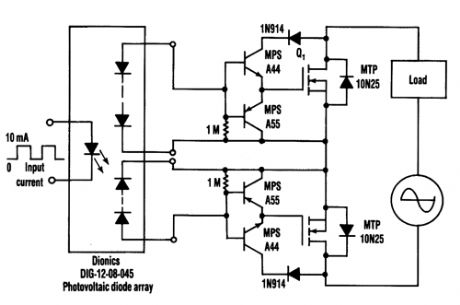

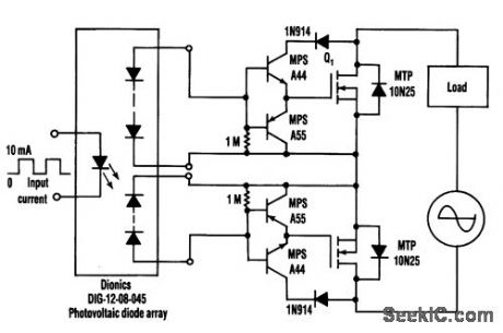
A clean and inexpensive way to eliminate the floating-gate supply is to use the voltage available at the MOSFET's drain to drive its gate. Tying the collector of Q1(a high-voltage, small-signal, 400-V NPN)to the MOSFET's drain supplies sufficient gate-drive voltage when it's needed most-when the MOSFET's drain-to-source voltage is high. Two such circuits used back-to-back form an ac relay.Using the emitter follower attached to the drain increases gate-drive current and decreases the MOSFET's turn-on time by a factor equal to the high-voltage NPN's beta. The resulting drain-to-source voltage fall times depend on the MOSFET's size and its required gate charge. The circuit that's used gives a fall time of 200 ps for an MTP10N2f5 10-A, 250-V MOSFET. With such fall times cutting switching losses, pulse-width modulation at frequencies under 100 Hz is possible.During tune-on, VDS falls rapidly until it reaches the sum of the 1N914 diode's 0.7-V drop, the collector-emitter saturation voltage of Q1, and the gate-to-source voltage required to support the load cur-rent. At that point, the diode array completes the MOSFET's turn-on, unaided by the buffer. This slows the fall of 7,s considerably when it reaches about 5 to 7 V. In high-voltage, low-frequency systems, tail-'ma of VDS is tolerable because the tail's voltage magnitude constitutes a small fraction of the switching voltage. The IN914 makes it possible for VGS to exceed VDS as the MOSFET completes turn-on. (View)
View full Circuit Diagram | Comments | Reading(3467)
SOLAR_POWER_SUPPLY
Published:2009/6/22 22:57:00 Author:May
This circuit delivers either 4.8 or 7.2 V regulated at 15 mA with a 3-V input from a bank of pho-tocells. R1 should be 453 kΩ for a 7.2-V output and 274 kΩ for a 4.8-Vdc output. Regulator efficiency is around 70%. This should be considered when selecting suitable solar cells. (View)
View full Circuit Diagram | Comments | Reading(802)
SELF_RETRIGGERING_TIMED_ON_GENERATOR
Published:2009/6/22 22:47:00 Author:Jessie

When power is first applied to the circuit, CZ begins to charge via LED1, R3, and R4. When the voltage across C2 reaches UI's input trigger level, the output of UI at pin 6 goes positive for a period that is determined by the values of C1 and R1. That turns Q1 on, discharging C2 through Dl and Q1.
At the end of the set period, the output of UI at pin 6 goes low, turning Q1 off and allowing the current to begin flowing through LED1, R3, and R4 to gain charge C2, causing the cycle to repeat.The repeat time is determined by the values of R3, R4, and C2. The previous formula won't be as accurate for this circuit, but it will at least get you close enough for the capacitor value; then R4, can be fine-tuned to obtain the desired timing period. (View)
View full Circuit Diagram | Comments | Reading(1472)
SUN_TRACKING_CIRCUIT_FOR_SOLAR_ARRAYS
Published:2009/6/22 22:38:00 Author:May
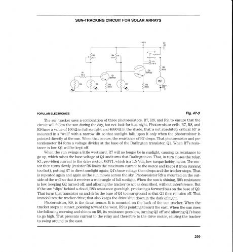
The sun tracker uses a combination of three photoresistors. R7, R8, and R9, to ensure that the circuit will follow the sun during the day, but not look for it at night. Photoresistor cells, R7, R8, and R9 have a value of 160Ω in full sunlight and 4880 Ω in the shade, that is not absolutely critical. R7 is mounted in a well with a narrow slit so that sunlight falls upon it only when the photoresistor is pointed directly at the sun. When that occurs, the resistance of R7 drops. That photoresistor and potentiometer R4 form a voltage divider at the base of the Darlington transistor, Q1. When R7's resistance is low, Q1 will be kept off.
When the sun swings a little westward, R7 will no longer be in sunlight, causing its resistance to go up, which raises the base voltage of Q1 and turns that Darlington on. That, in turn closes the relay, K1, providing current to the drive motor, MOT1, which is a 1.5-Vdc, low-torque hobby motor. The motor then turns slowly (resistor R6 limits the maximum current to the motor and keeps it from running too fast), putting R7 in dire'ct sunlight again; Q1's base voltage then drops and the tracker stops. That is repeated again and again as the sun moves across the sky. Photoresistor R8 is mounted on the outside of the well so that it receives a wide angle of full sunlight. When the sun is shining, R8's resistance is low, keeping Q2 turned off, and allowing the tracker to act as described, without interference. But if the sun slips behind a cloud, R8's resistance goes high, producing a forward bias on the base of Q2.That turns that transistor on and sinks the base of Q1 to near ground so that Q1 then remains off. That immobilizes the tracker drive; that also keeps the drive shut down in the dark of night.
Photoresistor, R9, is the dawn sensor. It is mounted on the back of the sun tracker. When the tracker stops at sunset, pointing toward the west, R9 is pointing toward the east. When the sun rises the following morning and shines on R9, its resistance goes low, turning Q2 off and allowing Q1's base to go high. That presents current to the relay and therefore to the drive motor, causing the tracker to swing around to the east. (View)
View full Circuit Diagram | Comments | Reading(5138)
LASER_dc_SUPPLY
Published:2009/6/22 22:33:00 Author:May
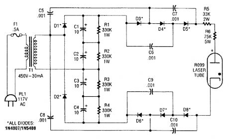
The supply provides about 6 kVdc when open circuited, dropping to around 1375 Vdc when loaded. The R099 is a laser tube. (View)
View full Circuit Diagram | Comments | Reading(865)
BATTERY_CONDITION_INDICATOR_FOR_12_V_BATTERIES
Published:2009/6/22 22:30:00 Author:May
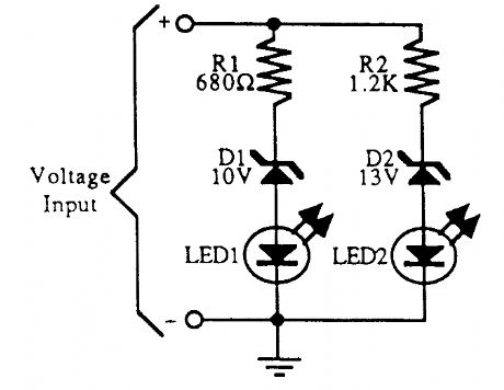
A simple battery condition indicator. Choose the Zener diodes to provide a window for over/un-der voltage indication. (View)
View full Circuit Diagram | Comments | Reading(1920)
LITHIUM_MEMORY_BACKUP_BATTERY_REPLACEMENT
Published:2009/6/22 22:30:00 Author:May
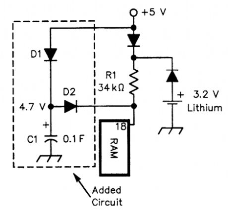
Physically very small high-capacitance capacitors are available for memory backup. Here, a 0.1-F (100,000μF) capacitor and two diodes replace the lithium battery. The lithium battery can be re-tained as well, providing double backup. (View)
View full Circuit Diagram | Comments | Reading(1285)
| Pages:177/291 At 20161162163164165166167168169170171172173174175176177178179180Under 20 |
Circuit Categories
power supply circuit
Amplifier Circuit
Basic Circuit
LED and Light Circuit
Sensor Circuit
Signal Processing
Electrical Equipment Circuit
Control Circuit
Remote Control Circuit
A/D-D/A Converter Circuit
Audio Circuit
Measuring and Test Circuit
Communication Circuit
Computer-Related Circuit
555 Circuit
Automotive Circuit
Repairing Circuit