
power supply circuit
Index 5
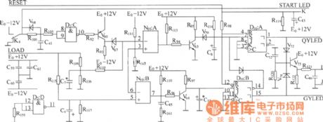
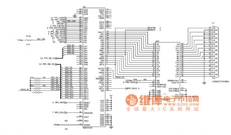
CASPER TM-5154HY type multi-frequency color monitor power supply circuit
Published:2014/2/26 20:41:00 Author:lynne | Keyword: CASPER TM-5154HY type multi-frequency color monitor power supply circuit,
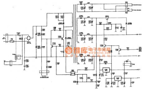
CASPER TM-5154HY type multi-frequency color monitor power supply circuit shown in Figure:
(View)
View full Circuit Diagram | Comments | Reading(1574)
Electro-optical distance transmitter circuit diagram
Published:2014/2/26 20:31:00 Author: | Keyword: Electro-optical distance transmitter circuit diagram,

Electro-optical distance transmitter circuit diagram
(View)
View full Circuit Diagram | Comments | Reading(1493)
To hear type light detector circuit diagram
Published:2014/2/26 20:18:00 Author: | Keyword: To hear type light detector circuit diagram,
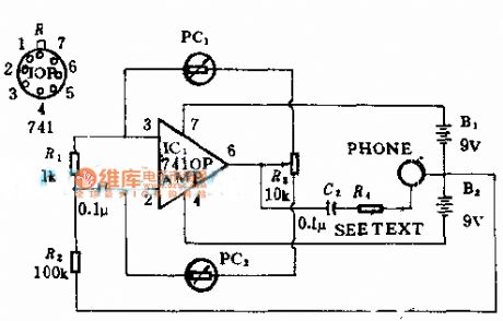
To hear type light detector circuit diagram
(View)
View full Circuit Diagram | Comments | Reading(1231)
SGH - P408 troubleshooting and circuit principle diagram _22
Published:2014/2/25 21:05:00 Author: | Keyword: SGH - P408 troubleshooting and circuit principle diagram _22,
SGH as shown - P408 troubleshooting and circuit principle diagram _22 (View)
View full Circuit Diagram | Comments | Reading(1212)
SGH - P408 troubleshooting and circuit principle diagram _24
Published:2014/2/25 20:55:00 Author: | Keyword: SGH - P408 troubleshooting and circuit principle diagram _24
SGH as shown - P408 troubleshooting and circuit principle diagram _24 (View)
View full Circuit Diagram | Comments | Reading(1252)
Mazda starting circuit diagram (MT)
Published:2014/2/24 21:55:00 Author: | Keyword: Mazda starting circuit diagram (MT),
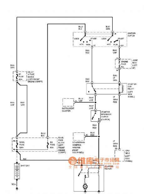
Mazda starting circuit diagram as shown (MT) (View)
View full Circuit Diagram | Comments | Reading(1364)
Figure 02 ICETEK C6711 - A principle
Published:2014/2/24 21:54:00 Author: | Keyword: Figure 02 ICETEK C6711 - A principle,
ICETEK - C6711 - A principle as shown in figure 02 (View)
View full Circuit Diagram | Comments | Reading(1196)
The light to change detector relay circuit diagram
Published:2014/2/24 21:53:00 Author: | Keyword: The light to change detector relay circuit diagram,
The light to change detector relay circuit diagram
(View)
View full Circuit Diagram | Comments | Reading(1392)
Test probe circuit diagram
Published:2014/2/24 21:52:00 Author: | Keyword: Test probe circuit diagram,

Test probe circuit diagram
(View)
View full Circuit Diagram | Comments | Reading(1306)
ICETEK C6711 -- A schematic 03
Published:2014/2/24 21:51:00 Author: | Keyword: ICETEK C6711 -- A schematic 03,
ICETEK - C6711 - A principle as shown figure 3 (View)
View full Circuit Diagram | Comments | Reading(1267)
DZW75-48/50 (ii) 50 reset control circuit diagram
Published:2014/2/24 21:45:00 Author: | Keyword: DZW75-48/50 (ii) 50 reset control circuit diagram,
View full Circuit Diagram | Comments | Reading(1337)
Logic probe circuit diagram
Published:2014/2/24 21:43:00 Author: | Keyword: Logic probe circuit diagram,
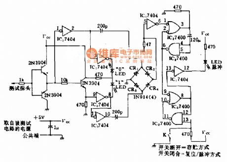
Logic probe circuit diagram
(View)
View full Circuit Diagram | Comments | Reading(1848)
ICETEK C6711 -- A schematic diagram 4
Published:2014/2/24 21:40:00 Author: | Keyword: ICETEK C6711 -- A schematic diagram 4,
As shown in figure ICETEK C6711 -- A principle diagram 4 (View)
View full Circuit Diagram | Comments | Reading(755)
DZW75-48/50 (ii) 50 are filled, floating conversion circuit diagram
Published:2014/2/24 21:24:00 Author: | Keyword: DZW75-48/50 (ii) 50 are filled, floating conversion circuit diagram,
View full Circuit Diagram | Comments | Reading(747)
ICETEK C6711 -- A schematic 05
Published:2014/2/24 21:17:00 Author: | Keyword: ICETEK C6711 -- A schematic 05,

As shown ICETEK C6711 -- A schematic 05 (View)
View full Circuit Diagram | Comments | Reading(819)
DZW75-48/50 (50 ii) voltage and current limit, flow diagram
Published:2014/2/23 21:27:00 Author: | Keyword: DZW75-48/50 (50 ii) voltage and current limit, flow diagram,
View full Circuit Diagram | Comments | Reading(860)
ICETEK C6711 -- A principle diagram of 06
Published:2014/2/23 21:25:00 Author: | Keyword: ICETEK C6711 -- A principle diagram of 06,
As shown in figure ICETEK C6711 -- A principle diagram of 06 (View)
View full Circuit Diagram | Comments | Reading(774)
Blown fuse flash circuit diagram
Published:2014/2/23 21:24:00 Author: | Keyword: Blown fuse flash circuit diagram,
Blown fuse flash circuit diagram
(View)
View full Circuit Diagram | Comments | Reading(884)
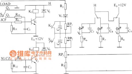
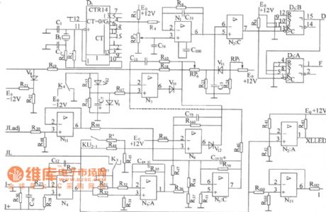
DZW75-48/50 (ii) 50 high-frequency rectifier filter circuit diagram
Published:2014/2/23 21:18:00 Author: | Keyword: DZW75-48/50 (ii) 50 high-frequency rectifier filter circuit diagram,
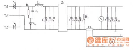
High-frequency transformer T secondary induction of positive and negative pulse of alternating voltage, after composed of high-power high-frequency switching diode V1 and V2 full-wave rectifier rectifier, repass L1 inductor and capacitor C2, C3 and C4 L filter and Z1 power filter consisting of smoothing filtering, such as on the output side for high frequency noise in accordance with the requirements of the indicators of 48 v dc voltage output. Pulse width directly decided to the discretion of the output voltage. Pulse width is wide, the output voltage is high, narrow pulse width, low output voltage. On the output side and a voltmeter, to display the output dc voltage measurement. R2 for discharge resistance, FL for shunt, a current meter jumper on both ends of FL to measure shows that the output of the rectifier current value, voltage value at the ends of the FL also as output current sampling signal to the voltage and current limit, flow circuit. R1, C1 and V3 RCD absorbing circuit to absorb the secondary voltage overshoot. (View)
View full Circuit Diagram | Comments | Reading(866)
The trigger drive SCR flash circuit diagram
Published:2014/2/23 21:13:00 Author: | Keyword: The trigger drive SCR flash circuit diagram,
The trigger drive SCR flash circuit diagram
(View)
View full Circuit Diagram | Comments | Reading(1212)
| Pages:5/291 1234567891011121314151617181920Under 20 |
Circuit Categories
power supply circuit
Amplifier Circuit
Basic Circuit
LED and Light Circuit
Sensor Circuit
Signal Processing
Electrical Equipment Circuit
Control Circuit
Remote Control Circuit
A/D-D/A Converter Circuit
Audio Circuit
Measuring and Test Circuit
Communication Circuit
Computer-Related Circuit
555 Circuit
Automotive Circuit
Repairing Circuit