
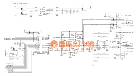
power supply circuit
Index 6
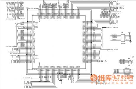
ICETEK 07 - C6711 - A schematic diagram
Published:2014/2/23 21:12:00 Author: | Keyword: ICETEK 07 - C6711 - A schematic diagram,
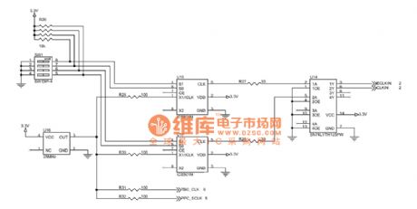
As shown in figure ICETEK 07 - C6711 - A schematic diagram (View)
View full Circuit Diagram | Comments | Reading(762)
1.5 v led flash circuit diagram
Published:2014/2/23 21:10:00 Author: | Keyword: 1.5 v led flash circuit diagram,
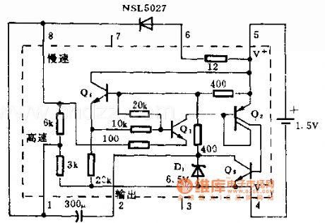
1.5 v led flash circuit diagram
(View)
View full Circuit Diagram | Comments | Reading(1112)
Order book flash communication circuit diagram
Published:2014/2/23 21:08:00 Author: | Keyword: Order book flash communication circuit diagram,
Order book flash communication circuit diagram
(View)
View full Circuit Diagram | Comments | Reading(928)
DZW75-48/50 (ii) 50 drive circuit diagram
Published:2014/2/23 21:04:00 Author: | Keyword: DZW75-48/50 (ii) 50 drive circuit diagram,
View full Circuit Diagram | Comments | Reading(833)
ICETEK C6711 -- A principle chart 08
Published:2014/2/23 21:01:00 Author: | Keyword: ICETEK C6711 -- A principle chart 08,
As shown in figure ICETEK C6711 -- A principle chart 08 (View)
View full Circuit Diagram | Comments | Reading(864)
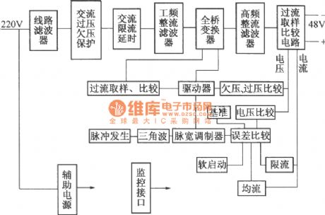
DZW75-48/50 (ii) 50 input circuit diagram
Published:2014/2/23 20:51:00 Author: | Keyword: DZW75-48/50 (ii) 50 input circuit diagram,
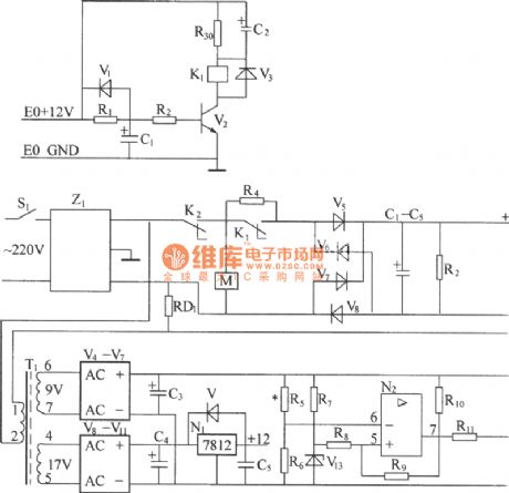
(1) 220 v AC voltage (50 hz) after Z1 line filter filter to AC overvoltage, undervoltage protection relay K2 contact, K2 contacts shall be closed up in normal working conditions, the AC voltage from 220 v AC current limiting resistor R4 R4 (after startup delay a period of time by K1 contact nipple), sent to the bridge rectifier rectifier power frequency, after smoothing filter and capacitor group about the output voltage of the DC 300 v, AC/DC power frequency conversion. R2 for discharge resistor. (2) the Z1 line filter is used to suppress and absorption power grid may have strong pulse interference with rectifier, improve the reliability of the rectifier. Line filter is good at the same time the common mode and differential mode of insertion loss, can effectively suppress the high frequency switch converter produced by reverse output of high frequency interference signals, the rectifier and isolation of power network, avoid mutual interference. (3) ac overvoltage, undervoltage protection circuit, ac 220 v voltage of line filter filter to the step-down transformer. (4) ac current limit delay circuit, ac voltage within the normal working range can be connected to the machine, ac power after the access time in auxiliary power supply, and after the construction of the auxiliary power supply by time delay, to make communication sub resistor, this paragraph of time is called ac current limit delay, it is being done by the alternating current limit delay circuit. (View)
View full Circuit Diagram | Comments | Reading(855)
ICETEK C6711 -- A schematic 09
Published:2014/2/23 20:45:00 Author: | Keyword: ICETEK C6711 -- A schematic 09,
As shown in figure ICETEK C6711 -- A schematic 09 (View)
View full Circuit Diagram | Comments | Reading(816)
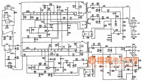
SUPERSYNC MD-10III, 1290, 1293, six kinds of power supply circuit diagram for the color display
Published:2014/2/23 20:48:00 Author:lynne | Keyword: SUPERSYNC MD-10III, 1290, 1293, six kinds of power supply circuit diagram for the color display,
SUPERSYNC MD-10III, 1290, 1293, six kinds of power supply circuit diagram for the color display as shown:
(View)
View full Circuit Diagram | Comments | Reading(1010)
SUPERSYNC MD-11III、1369、1505, the power of the three models of color display circuit diagram
Published:2014/2/23 20:46:00 Author:lynne | Keyword: SUPERSYNC MD-11III、1369、1505, the power of the three models of color display circuit diagram,
SUPERSYNC MD-11III、1369、1505, the power of the three models of color display circuit diagram as shown:
(View)
View full Circuit Diagram | Comments | Reading(862)
SUPERSYNC PWB - 1537 and EM - 1428 model two kinds of color display of power supply circuit diagram
Published:2014/2/23 20:19:00 Author:lynne | Keyword: SUPERSYNC PWB - 1537 and EM - 1428 model two kinds of color display of power supply circuit diagram,
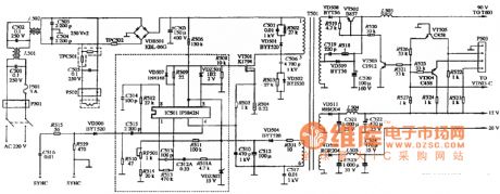
SUPERSYNC PWB - 1537 and EM - 1428 model two kinds of color display of power supply circuit diagram as shown:
(View)
View full Circuit Diagram | Comments | Reading(1004)
DZW75-48/50 (type ii) 50 rectifier module principle circuit diagram
Published:2014/2/19 21:15:00 Author: | Keyword: DZW75-48/50 (type ii) 50 rectifier module principle circuit diagram,
DZW75 type series switch rectifier module technical performance is as follows: (1) voltage regulation accuracy: < plus or minus 0.5% : (2) the noise voltage: (1) telephone scale heavy noise voltage < 2 mv < 200 mv (3) (2) a peak peak noise voltage broadband noise < 100 mv (3.4 kHz to 150 kHz) < 20 mv (0.15 MHz ~ 30 MHz) (4) discrete noise < 5 mv (3.4 kHz to 150 kHz) < 3 mv (150 kHz to 200 kHz) < 2 mv (200 kHz to 500 kHz) 85%; (4) power factor: > 85% (DZW75-48/50 ii was 99%); (5) load split: plus or minus 0.5% or less: (6) with jump machine overvoltage, undervoltage, over current protection, soft start boot function; (7) has a remote control, remote communication, remote sensing interface; (8) with independent work/involuntary way to work. (View)
View full Circuit Diagram | Comments | Reading(952)
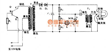
Thyristor drive save tube led flash circuit diagram
Published:2014/2/19 21:15:00 Author: | Keyword: Thyristor drive save tube led flash circuit diagram,
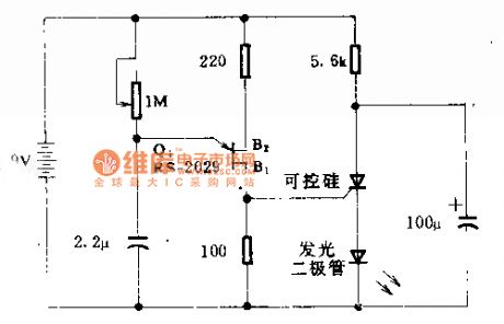
Thyristor drive save tube led flash circuit diagram
(View)
View full Circuit Diagram | Comments | Reading(990)
Xenon flash light circuit diagram
Published:2014/2/19 21:11:00 Author: | Keyword: Xenon flash light circuit diagram,
Xenon flash light circuit diagram
(View)
View full Circuit Diagram | Comments | Reading(1749)
500 candela flash circuit diagram
Published:2014/2/19 21:08:00 Author: | Keyword: 500 candela flash circuit diagram,
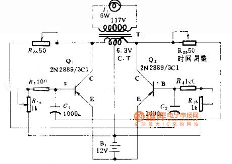
500 candela flash circuit diagram
(View)
View full Circuit Diagram | Comments | Reading(1018)
The basic principle of static switch circuit diagram
Published:2014/2/19 21:02:00 Author: | Keyword: The basic principle of static switch circuit diagram,
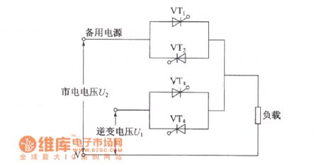
The effect of static switch: two ac power frequency and amplitude are just can work in parallel at the same time. When an ac power failure occurs, will produce a balance between the two power supply current, so that the change of two parallel power supply output voltage, affect the reliability of power supply. Static switch is used to cut off the power source of the failure of the output, achieve the inverter output and uninterrupted switch between the mains bypass output. For less than 2 kva on-line UPS power supply, the inverter output and mains bypass output q switch, USES fast relay as switching elements, mostly because of the switching time is only 2 ~ 5 ms, ms to fit the needs of communication equipment for power don't interrupt. For capacity in more than 2 kva UPS power supply, due to the relay working current increases, the switch time will increase to 80 ms to 120 ms, and snap relay instant sparks will produce high temperature and damage the contact, or often opened in electric arc is formed between the normally closed contacts and will have a instantaneous short circuit, two ac power, so relay used in switching is limited to small capacity of UPS power supply. Ac double contactor with interlock properties, although can control the output power larger UPS power supply, but the switch time has more than 10 milliseconds. (View)
View full Circuit Diagram | Comments | Reading(1005)
In line with the discriminator circuit diagram
Published:2014/2/19 21:00:00 Author: | Keyword: In line with the discriminator circuit diagram,
In line with the discriminator circuit diagram
(View)
View full Circuit Diagram | Comments | Reading(913)
Santana 2000 car engine room wiring harness layout diagram
Published:2014/2/19 20:36:00 Author: | Keyword: Santana 2000 car engine room wiring harness layout diagram,
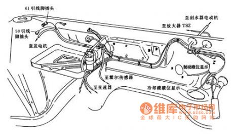
Santana 2000 car engine room as shown wiring harness layout diagram (View)
View full Circuit Diagram | Comments | Reading(1094)
ICETEK C6711 - A principle in figure 10
Published:2014/2/19 20:35:00 Author: | Keyword: ICETEK C6711 - A principle in figure 10,
ICETEK - C6711 - A principle as shown in figure 10 (View)
View full Circuit Diagram | Comments | Reading(839)
Set the static switch type single phase transformation of UPS power main circuit frame diagram
Published:2014/2/19 20:32:00 Author: | Keyword: Set the static switch type single phase transformation of UPS power main circuit frame diagram,
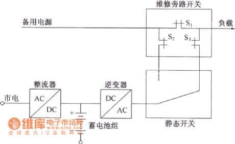
UPS power inverter based on combination can be divided into the transformation type and model, set up the static switch type single phase transformation of UPS power main circuit diagram as shown. The figure shows that when the mains is normal, for the inverter output as the main power supply load. In order to facilitate maintenance, set up a manual maintenance bypass switch, namely access to bypass switch S, closed, and then make the S2, S3 and static switch. Under standby power supply power to the load, the UPS system away from the bypass system, which can do maintenance of inverter, static switch. When the inverter as primary power supply, first close the static switch and the bypass switch S2, S3, and then disconnect S1. (View)
View full Circuit Diagram | Comments | Reading(1016)
The ladder wave inverter output three-phase transformer winding connection circuit diagram and the output voltage waveform
Published:2014/2/19 20:23:00 Author: | Keyword: The ladder wave inverter output three-phase transformer winding connection circuit diagram and the output voltage waveform,
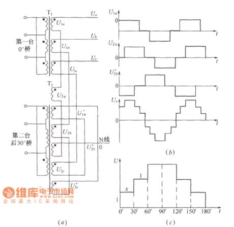
As shown in figure, (a) the ladder wave inverter for three-phase output transformer winding connection; (b) the output waveform. (View)
View full Circuit Diagram | Comments | Reading(2766)
| Pages:6/291 1234567891011121314151617181920Under 20 |
Circuit Categories
power supply circuit
Amplifier Circuit
Basic Circuit
LED and Light Circuit
Sensor Circuit
Signal Processing
Electrical Equipment Circuit
Control Circuit
Remote Control Circuit
A/D-D/A Converter Circuit
Audio Circuit
Measuring and Test Circuit
Communication Circuit
Computer-Related Circuit
555 Circuit
Automotive Circuit
Repairing Circuit