
Basic Circuit
Index 282
JOGGER_DATA_COLLECTlON
Published:2009/7/3 3:01:00 Author:May
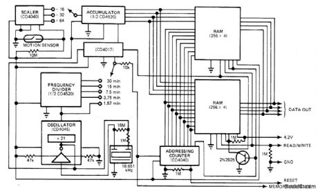
Portable data acquisition system using microcomputer to drive digital cassette tape transport operates from 12-V rechargeable battery and fits in backpack having total weight of only 8 Ib. Sample rate can be set between 20 and 100 Hz, with 2 min of continuous data being stored at fast rate. Recorded data is played into PDP-11 minicomputer later for analysis. Motion sensor shown can be replaced by other types of transducers for mea uring desired physiological phenomena during jogging, walking, or running.-P. G. Schreier, Physiological Data Acquisition Presents Unusual Problems, Solutions, EDN Magazine, June 20, 1978, p 25-26, 28, and 30. (View)
View full Circuit Diagram | Comments | Reading(749)
Cable_length
Published:2009/7/23 23:42:00 Author:Jessie
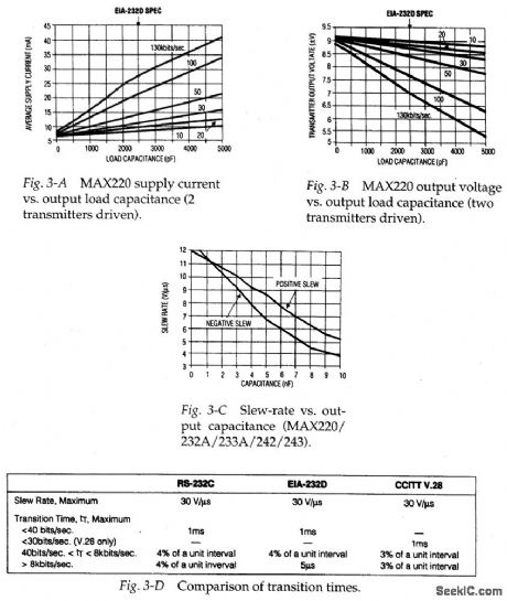
The old RS-232C interface specification calls for a maximum cable length of 50 feet.The newer EIA-232D specification calls for a length of cable that produces a capacitance of 2500 pF. This change from feet of cable to pF of load capacitance recognizes one of the problems in RS-232C. Not only does RS-232C ignore the effects of cable capacitance, but it contains a 50-ft distance limit that is often ignored by designers.
The EIA-232D specification considers cable length indirectly, through the effect of load capacitance, but does not specify a maximum length. Because the capacitance of inexpensive cable can range from 12 pF/ft for a single twisted pair to 30 pF/ft for low-noise shielded, multiple-twisted-pair cable, there is some confusion.
Cable capacitance is important because EIA-232D transmission are ac signals. Higher capacitance demands higher peak currents from the transmitter, resulting in higher average supply current for a given data rate, as shown in Fig. 3-A. Also, the cable impedance forms an ac divider with the transmitter output impedance. Higher cable capacitance lowers the divider shunt component. In turn, this reduces signal amplitude at the receiver end of the cable, as shown in Fig. 3-B. This signal loss becomes a problem when the receiver-end voltage falls below the specified 5-V minimum input level (required by most digital equipment).
Finally, cable capacitance limits the slew rate available from a given transmitter, as shown in Fig. 3-C. The slew rate determines the transition time between the +3-V and -3-V signal levels. (Slew rate is discussed further in Chapter 6.) Transition time limits the maximum data rate according to the specifications in RS-232C, EIA-232D, and CCITT V28, as shown in Fig. 3-D.
The simplest way to calculate the maximum allowable cable length for an EIA-232D interface IC (transceiver) is to divide the 2500-pF load specification by the capacitance per foot specified for the cable. Then, for cable lengths up to that limit, you can rest assured that the transceiver will operate properly and provide the maximum specified data rate.
Figure 3-E shows how the data rate can be extended past the specification limits. Longer cable adds to the line capacitance, lengthening the signal transition time, thus limiting the data rate. However, you can implement cable lengths and data rates well beyond the limits implied by the EIA-232D specification. (View)
View full Circuit Diagram | Comments | Reading(804)
300_3000_Hz_TUNABLE_FOUR_FUNCTION
Published:2009/7/3 3:00:00 Author:May
Provides choice of high-pass, bandpass, low-pass, and tunable notch outputs. Uses National LM324 quad opamp. Tuning pots are ganged 500K 2-W carbon with reverse log taper. Notch of -35 dB is 200 Hz wide at -3 dB points. Notch output has unity gain with respect to input signal, but other three outputs provide gain.-P.A. Lovelock, Discrete Operational Amplifier Active Filters, Ham Radio, Feb.1978, p 70-73. (View)
View full Circuit Diagram | Comments | Reading(1707)
700_2000_Hz_TUNABLE_BANDPASS
Published:2009/7/3 2:58:00 Author:May
Uses RC notch circuit as feedback element for active-filter opamp. With tuning pot set for center frequency of 1000 Hz, 3-dB bandwidth is 23 Hz and 10-dB bandwidth is 68 Hz. At 1000 Hz, voltage gain is 36 dB. High-frequency rolloff is good, being 43 dB down at 2000 Hz, so circuh converts 1000-Hz square wave into sine wave. Artide gives design equations.-C. Hall, Tunable RC Notch Filter, Ham Radio, Sept. 1975, p 16-20. (View)
View full Circuit Diagram | Comments | Reading(1284)
10_MHz_TRACKING
Published:2009/7/3 2:58:00 Author:May
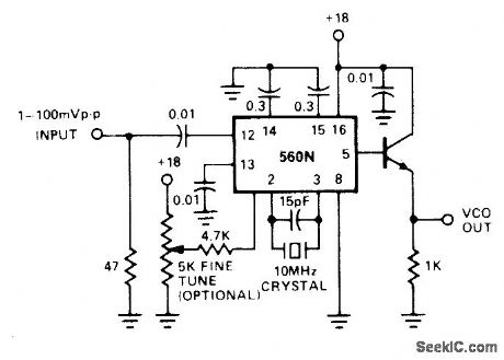
Connection shown for 560N PLL tracking filter uses crystal to keep free-runnlng frequency at desired value for Signals near 10 MHz Lock range varies with inputamplitude,from about 0.3 kHz for 1 mV P-P input to about 3 kHz for 100 mV P-P.- Signetics Analog Data Manual, signetics,Sunnyvale,CA,1977,p 850-851. (View)
View full Circuit Diagram | Comments | Reading(854)
BANDPASS_FOR_CW
Published:2009/7/3 2:57:00 Author:May
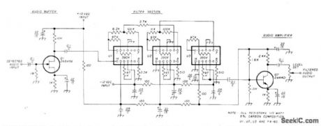
Sophisticated audio processing system for CW bandpass, using communication receiver, has actual bandpass center frequency between 900 and 950 Hz.Bandwidth is about 150 Hz Minimum relative attenuation is above 20 dB,Uses three KineticTechnology FX-60 ICs(cuned from FS-60,FS-65,and FS-61 production by manufacturer).-M. A.Chapman, Audio Filters for Improving SSB and CW Reception, Ham Radio, Nov.1976, p 18-23. (View)
View full Circuit Diagram | Comments | Reading(1432)
AUDIBLE_METER_READER
Published:2009/7/3 2:56:00 Author:May
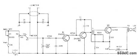
Analog meter terminals are connected to input of DC amplifier Q1 for feeding audio oscillator Q2 and output amplifier Q3. Frequency of oscillator is directly proportional to reading of meter. At calibrate position of S2, DC amplifier is fed by voltage divider R1-R2 and R2 is adjusted until tones heard are identical for both positions of S2. Developed for use by blind person. Knob of R2 sweeps over large scale having markings in Braille for reading of setting at which tones match. Alternatively, R2 can be preset to desired reading and equipment under test adjusted to give tone match. Article covers construction and calibration. C1 is chosen in range of 0.002 to 0.1 μF to give desired minimum fre quency. C2, if required, is in same range. T1 is transistor driver transformer (10,000 to 2000 ohms), and T2 is transistor output transformer (500 to 3.2 ohms).-N .Rosenberg, Tune-UpAids forthe Blind.73Magazine, Feb,1978,p64-67. (View)
View full Circuit Diagram | Comments | Reading(636)
05MHz_WITH_100_DEVIATION_
Published:2009/7/3 2:55:00 Author:May
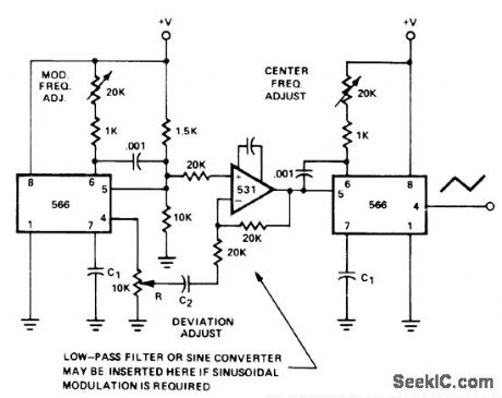
Carrier frequency under 0.5 MHz is generated by 566 function generator at right, for modulation by other 566 connected as triangle generator whose output is boosted by 531 opamp to give deviations up to ±100% of carrier frequency. Capacitors C1 control frequency range of each function generator.- Signetics Analog Data Manual, Signetics, Sunnyvale, CA, 1977, p 852-854. (View)
View full Circuit Diagram | Comments | Reading(1320)
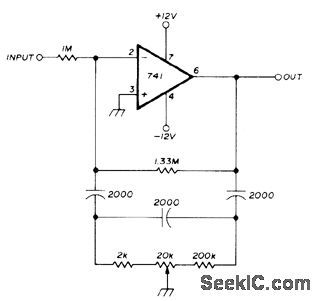
1_kHz_BANDPASS_NOTCH
Published:2009/7/3 2:54:00 Author:May
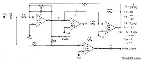


Biquad filter uses all four sections of LM324 quad differential-input opamp to provide choice of bandpass and notch outputs. Supply voltage range can be 3-32 v, with reference voltage equal to half of supply value used. For center frequency of 1 kHz,R is 160K, C is 0.001 μF, and R1-R3 are 1.6 megohms,Coupling capactions C1 can be 10 times value used for C.- Low Power Operational mplifiers, Motorola,Phoenix,AZ,1978,DS9339 R1. (View)
View full Circuit Diagram | Comments | Reading(1685)
SECOND_ORDER_1_kHz_LOW_PASS
Published:2009/7/3 2:52:00 Author:May
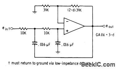
Circuit using 741 opamp has equalvalue series input resistors and high-pass capacitors. Cutoff frequency can be increased by changing 10K resistors to higher values while keeping their values identical. 10:1 resistance change provides 10:1 frequency change. Damping d is adjustable; critical value of 1.414 gives maximum flatness of response without overshoot. Interchange 10K resistors and 0.016-μF capacitors to convert circuit to 1-kHz high-pass filter.-D. Lancaster, Active-Filter Cookbook, Howard W. Sams, indianapolis, IN, 1975, p 127-129. (View)
View full Circuit Diagram | Comments | Reading(993)
DACs_with_high_voltage_and_high_current_outputs
Published:2009/7/25 5:37:00 Author:Jessie
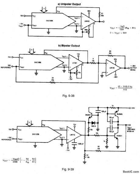
Figure 9-38 shows DAC1006s connected for high-voltage outputs, both unipolar and bipolar. The output current of these circuits depends on the current limit of the LM143 op amp (typically 20 mA). Figure 9-39 shows how a discrete power stage can be added to further increase output current capability (to 100 mA at 100 V). NATIONAL SEMICONDUCfOR, APPLICATION NOTE 271, 1994, P. 668. (View)
View full Circuit Diagram | Comments | Reading(801)
Capacitance_multiplier
Published:2009/7/25 5:35:00 Author:Jessie
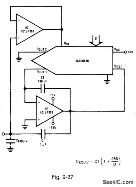
Figure 9-37 shows a DAC0830 connected as a capacitance multiplier,Actually, thecircuit is a DAC-controlled amplifier (used for capacitance multiplication) to give microprocessor control of system time-domain or frequency-domain response. The microprocessor controls the digital input to the DAC、which controls the amplifier to produce a variable capacitance,The capacitance can be used to varythe time constant of RC circuits varying either time or frequency.In this circuit the DAC adjusts the gam of a stage with fixed capacitive feedback. This produces aMiller-effect equivalent input capacitance equal to the fixed capacitance multiplied by 1 plus the amplifier gain.The voltage across the equivalent input capacitance to ground is limited to the maximum output voltage of op amp A1, divided by 1 plus 2n/D, where:n = the DAC bits of resolution, and D = decimal equivalent of the binary input. NATIONAL SEMICONDUCTOR, APPLICATION NOTE 271, P. 667.
(View)
View full Circuit Diagram | Comments | Reading(5350)
Decoded_Z80_interface
Published:2009/7/25 5:10:00 Author:Jessie
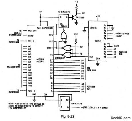
Figure 9-23 shows the ADC0816/17 connected to form a decoded 280 interface. A 6-bit comparator is used to decode A4 through A7 and IOREQ Two NOR gates are used to gate the ALE/START and OE pulses. This configuration functions the same as that of Fig. 9-22, except that the DM8131 provides much more decoding. NATIONAL SEMICONDUCTOR, APPLICATION NOTE 258, 1994, P. 608.
(View)
View full Circuit Diagram | Comments | Reading(774)
600_Hz_THIRD_ORDER__LOW_PASS
Published:2009/7/3 2:51:00 Author:May
Butter-worth filtor using 741 or equivalent opamp provides gain of 6 dB in passband below 600-Hz cutoff,All components can be 5% tolerance.- H.M.Berlin, Design of Active Filters,with Experiments, Howard W Sams, Indianapolis, IN,1977,p 114-116. (View)
View full Circuit Diagram | Comments | Reading(807)
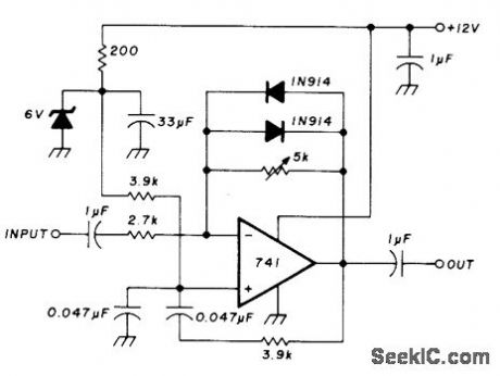
UART_FOR_EKG_RELAY
Published:2009/7/3 2:35:00 Author:May
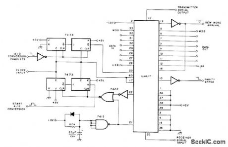
After electrocardiogram is converted to digital form by commercial A/D converter, circuit shown takes 8-bit word output of converter for processing by universal asynchronous receiver-transmitter (UART) to give required serial asynchronous code for transmitter of satellite relay system, with start, stop, and parity bits added to data under control of 19.2-kHz external clock. This serial output is then used to control FSK oscillator that switches between two discrete audio frequendes to give signal required for transmission through satellite. Article covers operation of UART in detail.-D. Nelson, Medical Data Relay via Oscar Satellite, Ham Radio, April 1977, p 67-73. (View)
View full Circuit Diagram | Comments | Reading(1031)
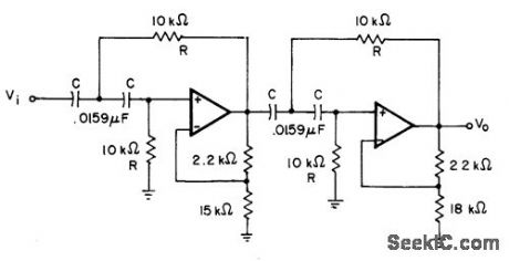
10_Hz_LOW_PASS
Published:2009/7/3 2:31:00 Author:May
Filter design for biomedical experiment has 10-Hz cutoff, tolerable transient and overshoot response, and at least 30-dB rejection of all frequencies above 15 Hz. All components should have 2% tolerance.-D. Lancaster, Active-Filter Cookbook, Howard W.Sams, lndianapolis, IN, 1975, p 147. (View)
View full Circuit Diagram | Comments | Reading(1169)
MEMORY_SAVE_ON_POWER_DOWN
Published:2009/7/3 2:25:00 Author:May
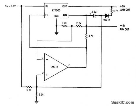
Circuit NotesThe auxiliary output powers the memory, while the main output powers the system and is connected to the memory store pin. When power goes down, the main output goes low, commanding the memory to store. The auxiliary output then drops out. (View)
View full Circuit Diagram | Comments | Reading(778)
18_19_MHz_BANDPASS
Published:2009/7/3 2:25:00 Author:May
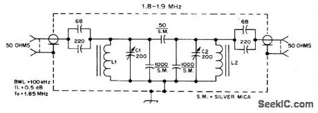
Butterwolth bandpass filter, suitable for use with broadband preamp, helps reject out-of-band signals. Filter also protects preamp from signals across response range from broadcast band through VHF. C1 and C2 are mica trimmers. L1 and L2 have 30 turns No. 22 enamel on Amidon T68-6 toroid cores to give 5.1 μH.-D. DeMaw, Beat the Noise with a Scoop Loop, QST, July 1977, p 30-34. (View)
View full Circuit Diagram | Comments | Reading(821)
800_Hz_BANDPASS
Published:2009/7/3 2:24:00 Author:May
Active filter has 800-Hz center frequency for optimum CW reception.Bandwidth is adjustable. Back-to-back diodes provide noise-limiting capability.-U. L. Rohde, IF Amplifier Design, Ham Radio, March 1977, p 10-21. (View)
View full Circuit Diagram | Comments | Reading(1116)
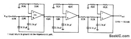
1_kHz_FOURTH_ORDER_HIGH_PASS
Published:2009/7/3 2:23:00 Author:May
First section is second-order high-pass filter having gain of 1.2 dB,and second section has gain of 7 dB Opamps are 741 or equivalent.-H.M.Berlin, Design of Active Filters, with Experiments, Howard W. Sams, Indianapolis, IN, 1977, p 116-117. (View)
View full Circuit Diagram | Comments | Reading(1304)
| Pages:282/471 At 20281282283284285286287288289290291292293294295296297298299300Under 20 |
Circuit Categories
power supply circuit
Amplifier Circuit
Basic Circuit
LED and Light Circuit
Sensor Circuit
Signal Processing
Electrical Equipment Circuit
Control Circuit
Remote Control Circuit
A/D-D/A Converter Circuit
Audio Circuit
Measuring and Test Circuit
Communication Circuit
Computer-Related Circuit
555 Circuit
Automotive Circuit
Repairing Circuit