
Basic Circuit
Index 297
LOW_COST_BAR_GRAPH_INDICATOR_FOR_AC_SIGNALS
Published:2009/7/1 22:15:00 Author:May
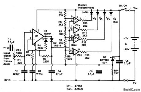
Indicator was designed for displaying the peak level of small ac signals from a vanety of transducers including microphones,stram gauges and photodiodes.The circuitresponds to input signals contained within the audio frequency spectrum, i.e.,30 Hz to 20 kHz,although a reduced response extends up to 40 kHz.Maximum sensitivityfor the component values shown,with VR1 fully clockwise,IS 30 mV peak-to-peak.The indicator can be calibrated by setting VR1 when an appropriate input signal is applied. (View)
View full Circuit Diagram | Comments | Reading(917)
TACHOMETER_WITCH_SOUARE_WAVE_OUT_PUT
Published:2009/7/1 22:11:00 Author:May
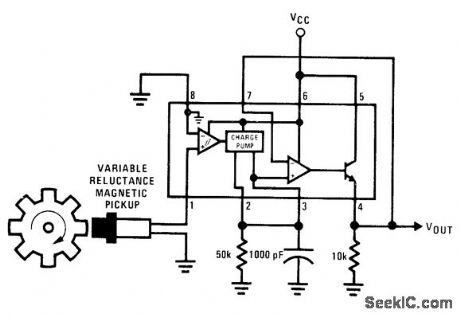
National LM2907 tachometerIC providessquare-wave output at same frequency as sine wave generated by magnetic pickup,for use asline driver in automatic control system.-″Linear Applications,vol .2, National Semiconductor、Santa Clara、CA、1976,AN-162,p12-13. (View)
View full Circuit Diagram | Comments | Reading(1137)
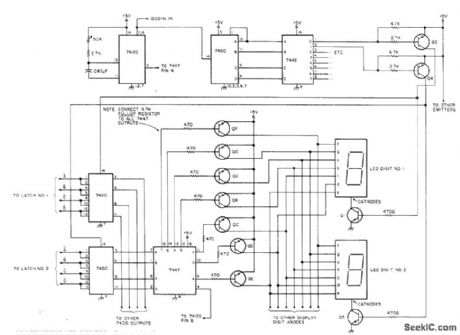
MULTIPLEXING_7_DIGITS
Published:2009/7/1 22:10:00 Author:May
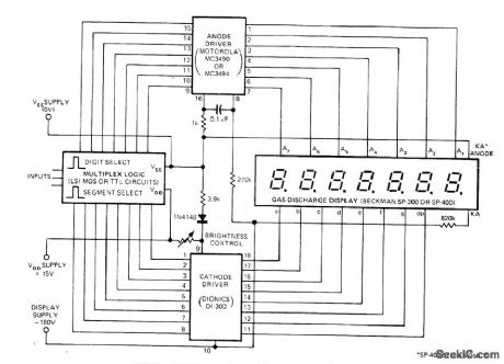
Uses Motorola MC3490 anode driver for active-high inputs (MC3494 for active-Iow inputs) to accept digitselect signals from multiplex logic source and drive display anodes directly. Constant cathode currents are maintained for gas-discharge display by Bionics Dl-300 IC, to provide constant brightness without using supply-voltage reguIation. For each digit added to display, equal number of anode drivers is required. Only one cathode driver is needed because all cathodes are bused together.-D. Sien, Multiplex Display Circuit Features Minimum Parts Count, EDN Magazine, May 5,1977, p 112. (View)
View full Circuit Diagram | Comments | Reading(739)
5_min_SHUTOFF
Published:2009/7/1 22:10:00 Author:May
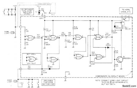
Vehicleintrusion alarm shuts off automatically in about 5 min after being triggered, as required by law in some states. Drain on battery is negligible until alarm is set off by intruder. Once triggered, operation sequence is not affected by subsequent opening or closing of doors. System uses two CMOS CD4001AE quad two-input NOR gates for switching logic. IC1 provides sensor interface, latch, and entry/exit time delays. IC2 provides output through Q1 amd relay, as well as automatic shutoff delay. Article gives construction details and layout for printed-circuit board.-W. J. Prudhomme, Vehide Security Systems, 73 Magazine, Oct. 1977, p 122-125. (View)
View full Circuit Diagram | Comments | Reading(621)
EXPANDED_SCALE_METER_DOT_OR_BAR
Published:2009/7/1 22:09:00 Author:May
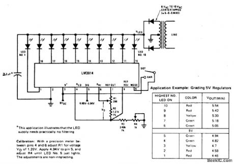
A bar graph driver IC LM314 drives an LED display.The LEDs may be separateor in a combined (integral) bar graph display. (View)
View full Circuit Diagram | Comments | Reading(3878)
VISUAL_INDICATOR
Published:2009/7/1 22:08:00 Author:May
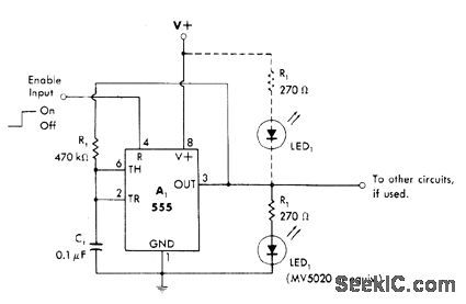
When circuit is activated by high output of burglar alarm circuit, 555 timer operating as very low frequency MVBR makes LED1 flash on and off during alarm condition. Alternate connection of LED1 to V+ holds LED1 on for standby while flashing it during alarm. Oscillator output is also available for other uses if desired. indicator can be located remotely from alarm.-W. G. Jung, IC Timer Cookbook, Howard W. Sams, Indianapolis, IN, 1977, p 232-235. (View)
View full Circuit Diagram | Comments | Reading(1025)
BCD_DECODER_2
Published:2009/7/1 22:08:00 Author:May
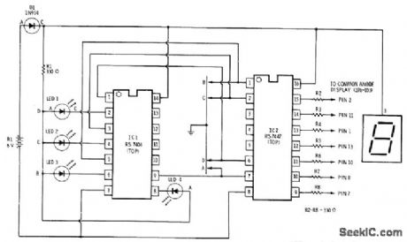
Drive for 7-segment commonanode digital display is provided by RS7447 BCD to 7-segment decoder. Binary input indicator using RS7404 hex inverter and four LEDs shows input in binary form for decimal digits 0-9. Developed for classroom demonstrations. Red LEDs can be Radio Shack 276-805,and display is 276-053,F.M.Mims, Integrated Circuit Projects,vol.6, Radio Shack,Fort Worth,TX,1977,p 42-52. (View)
View full Circuit Diagram | Comments | Reading(4944)
LITTLE_DIPPER
Published:2009/7/1 22:03:00 Author:May
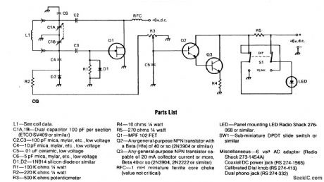
The circuit consists of two basic circuits, the oscillator and the detector. The oscillator uses an FET in a Colpitts configuration. The energy circulating in the oscillator tank is coupled through C4 to the detector circuit, where a small diode (D2) rectifies it, feeding a dc voltage to the Darlington pair (Q2, A3) con-trolled by the sensitivity control (R3). Any smallvariations in the bias of the amplifier will cause large variations of current through the LED indicator in the DiP mode; however, in the PEAK mode the current produces a corre-sponding voltage ropthrough R5 and the action of the LED is reversed. The circuit shown will work practically on any frequency from LF to VHF if the appropriate components are used. (View)
View full Circuit Diagram | Comments | Reading(947)
NOISE_SOURCE
Published:2009/7/1 21:52:00 Author:May
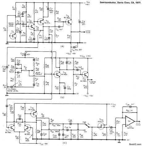
Used in synthesizer for generating wide variety of musical and other sounds, to provide any combination of white, filtered, and VLF noise to be used directly as audio signal or as control signal. Source for white noise is Tr1, which is a germanium transistor selected for high leakage or heated enough to make it leaky, so as to produce an average noise level of about 40 mV P-P. Filtered (colored) noise is produced by driving spec-trum-shaping network (Baxandall tone control) with white noise. Preset control R17. is adjusted so output shows no clipping when both red and blue tone controls are at maximum. VLF noise is extracted from white noise by either of two low-pass filters selected by S1. Three-part article describes operation in detailand gives all other circuits used in synthesizer-T. Orr and D. W. Thomas, Electronic Sound Synthesizer, Wireless World, Part 3-Oct. 1973, p 485-490 (Part 1-Aug. 1973, p 366-372; Part 2-Sept. 1973, p 429-434). (View)
View full Circuit Diagram | Comments | Reading(1155)
FUZZ_CIRCUIT
Published:2009/7/1 21:44:00 Author:May
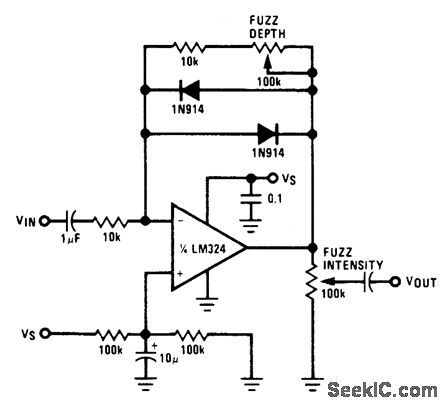
Two diodes in feedback path or LM324 opamp create musical-instrument effect known as fuzz by limiting output voltage swing to ±0.7 V. Resultant square wave contains chiefly odd harmonics, resembling sounds of clarinet. Fuzz depth pot controls level at which clipping begins, and fuzz intensity pot controls output level.- Audio Handbook, National Semiconductor. Santa Clara. CA. 1977. p 5-11. (View)
View full Circuit Diagram | Comments | Reading(3092)
MULTIPLEXING_LED_DRIVERS
Published:2009/7/1 21:41:00 Author:May
Duty cycle of each display digit can be varied from 10% (full on with strobing) to less than 1% (almost off).Circuit uses 7490 and 7442 as 1-of-10 multiplex driver to strobe cathodes of display digits through Q1, Q3, etc and tum on required 7400 multiplex gate through Q2, Q4, etc. Outputs of7447 are polarity-inverted by QA, QB, etc, which can be Sylvania ECG 159 rated at 200 mA. Q1,Q3, etc can be EGG 123 or HEP S0002, while Q2, Q4, etc can be any silicon PNP transistor.-B.Hart, Cument-Saver Counter Display, 73 Magazine, June 1977, p 174-176. (View)
View full Circuit Diagram | Comments | Reading(2353)
RANDOM_MUSIC
Published:2009/7/1 21:37:00 Author:May
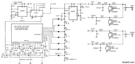
Uses Johnson counter as special shift register producing almost random bit patterns of 18 to 3255 12-bit words under control of clock operating in range of about 1-10 Hz. Oscillator (upper right) uses NE555 as voltage-controlled square-wave generator playing one of eight musical notes (C. D. E. F. G. A. B. or C), depending on state of seven noteselector lines coming from selector switches. Oscillator is divided down in frequency by three-stage ripple counter to provide four octaves of range. R1 -R8 serve fortuning each note to pitch. Outputs 8F and 2F are paired to drive left input of stereo amplifier, while outputs 16F and 4F are similarly paired for right channel. Article covers construction, tune-up, and creation of pleasing musicalsequences.-D. A. WalIace. The Sound of Random Numbers. 73 Mag-azine. Feb. 1976, p 60-64. (View)
View full Circuit Diagram | Comments | Reading(1036)
ELECTRONIC_FLASH_TRIGGER
Published:2009/7/1 21:35:00 Author:May
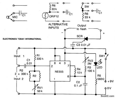
Circuit NotesA negative pulse at the input is fed via capacitor C1 to the input pin (2) of the IC.Pin 2 is held slightly above its triggering voltage of 1/3 Vcc, by the voltage divider comprising R1, R2 and RV1. The negative pulse triggers the IC and the output (pin 3) goes high for a time period controlled by RV2, R3 and C2. When the output goes low again at the end of the time interval, capacitor C3 charges through the gate cathode circuit of the SCR switching it on and firing the flash. Capacitor C1 isolates the input from the voltage divider so that the unit isn't sensitive to the dc level at the input. RV1 acts as a sensitivity control by allowing the voltage to be adjusted to a suitable level so that the input signal will trigger the IC. Resistor R4 limits the discharge current from C2 at the end of the timing cycle protecting the IC. The LED and its protective resistor R5 act as an indicator to show that the unit has triggered, simplifying the setting up process and minimizing the number of times the strobe has to be fired. This means that the strobe needn't be fired until a photo is to be taken. (View)
View full Circuit Diagram | Comments | Reading(870)
TTL_OSCILLATOR_INTERFACES_DATA_FOR_DISPLAY_BY_A_TELEVISION_SET
Published:2009/7/1 21:32:00 Author:May
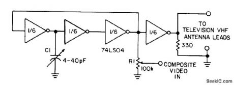
Three gates of a 74LS04 form the oscillator circuit. Capacitor C1 allows fine-frequency adjustment to a specific television channel and helps stabilize the circuit. Potentiometer R1 acts as the mixing input and provides adjustment of the contrast ratio for the best viewing. A fourth gate buffers and helps stabilize the oscillator. (View)
View full Circuit Diagram | Comments | Reading(700)
PlANO_MUSIC_FROM_ORGAN
Published:2009/7/1 21:29:00 Author:May

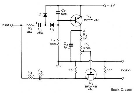
Simple add-on circuit for electronic organ attenuates output of oscillator exponentially to zero in manner suitable for mimicking waveform of piano. Circuit is self-triggering, so exponential decay starts only when output of multivibrator is applied; this eliminates need for extra contacts on key-board. With no input, Tr1 is on and point A is at supply voltage. Input signal turns Tr1 off, discharging C3 through R3 and R5. Voltage across C3 controls gate of FET, with R5 being adjusted so FET just switehes off when C3 is fully discharged. Tr1 then conducts and C3 charges rapidly, to permitfast piano playing.-C. J. Outlaw, Electronic Organ to Piano, Wireless World, Feb.1975, p 94. (View)
View full Circuit Diagram | Comments | Reading(1073)
DOUBLE_SIDEBANDSUPPRESSED_CARRIER_RF_MODULATOR
Published:2009/7/1 21:26:00 Author:May
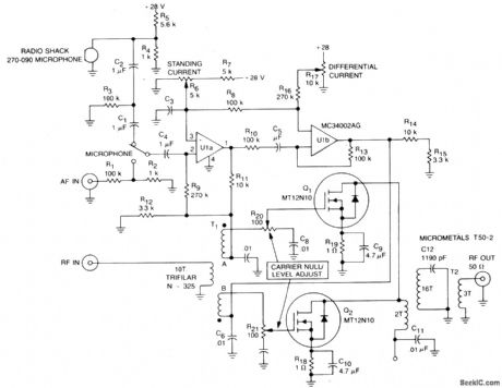
An RF input is applied to the primary of T1, which applies equal amplitude, opposite phase RF drive for output FETs Q1 and Q2. With no AF modulation at points A and B, the opposite phase RF signals cancel each other and no output appears at the 50 V output connector.When AF modulation is applied to points A and B, a modulated RF output is obtained. The dc stability and low frequency gain are improved by source resistors R18 and R19.A phase inverter consisting of a dual op amp (U1a and U1b) produces the out-of-phase, equal amplitude AF modulation signals. (View)
View full Circuit Diagram | Comments | Reading(835)
DC_STATIC_SWITCHSCR_FIIP_FLOP
Published:2009/7/1 21:24:00 Author:May
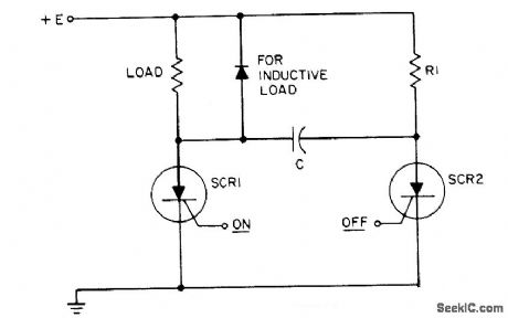
This circuit is a static SCR switch for use in a dc circuit. When a low power signal is applied to the gate of SCR1, this SCR is triggered and voltage is applied to the load.The right hand plate of C charges positively with respect to the left hand plate through R1. When SCR2 is triggered on, capacitor C is connected across SCR1, so that this SCR is momentarily reverse biased between anode and cathode. This reverse voltage turns SCR1 off provided the gate signal is not applied simultaneously to both gates. The current through the load will decrease to zero in an exponential fashion as C becomes charged. (View)
View full Circuit Diagram | Comments | Reading(2336)
NOISE_IMMUNE_60_Hz_LINE_SYNC
Published:2009/7/1 21:23:00 Author:May
View full Circuit Diagram | Comments | Reading(585)
POWER_ON_RESET
Published:2009/7/1 21:22:00 Author:May
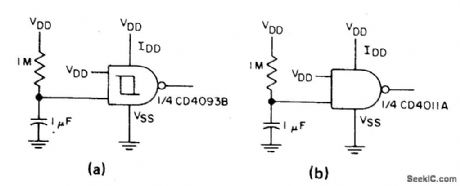
A reset pulse is often required at power-on in a digital system. This type of reset pulse is ideally provided by this circuit. Because of the high input imp-edance of the Schmitt trigger, long reset pulse times may be achieved without the excess dissipation that results when both output devices are on simultaneously, as in an ordinary gate device (B). (View)
View full Circuit Diagram | Comments | Reading(4387)
SHIFT_REGISTER
Published:2009/7/1 21:21:00 Author:May
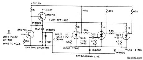
The shift pulse amplitude is less than 15 volts. If a stage is off, the shift pulse will no, be coupled to the next stage. If it is on, the diode will conduct triggering the next stage. Just prior to the shift pulse the anode supply is interrupted to turn off all stages.The stored capacitor charge determines which stages will be retriggered. (View)
View full Circuit Diagram | Comments | Reading(2622)
| Pages:297/471 At 20281282283284285286287288289290291292293294295296297298299300Under 20 |
Circuit Categories
power supply circuit
Amplifier Circuit
Basic Circuit
LED and Light Circuit
Sensor Circuit
Signal Processing
Electrical Equipment Circuit
Control Circuit
Remote Control Circuit
A/D-D/A Converter Circuit
Audio Circuit
Measuring and Test Circuit
Communication Circuit
Computer-Related Circuit
555 Circuit
Automotive Circuit
Repairing Circuit