
Basic Circuit
Index 295
AUDIO_FOR_COMPUTER_MUSIC
Published:2009/7/2 0:40:00 Author:May
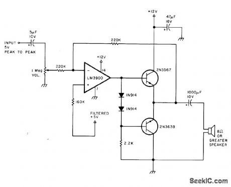
Wideband low-power audio amplifier was developed for use with DAC and low-pass active filter to create music with microprocessor.-H Chamberlin, A Sampling of Techniques for Computer Performance of Music, BYTE, Sept 1977, p 62-66、68-70, 72, 74, 76-80, and 82-83. (View)
View full Circuit Diagram | Comments | Reading(816)
TUNING_FOR_EQUAL_TEMPERAMENT
Published:2009/7/2 0:39:00 Author:May
Instrument described enables anyone to tune such instruments as organ, piano, and harpsichord in equal temperament with accuracy approaching that of professional tuner. Only requirement is ability to hear beats between two tones sounded together. Master oscillator circuit shown generates 250.830 kHz for feeding to first of five ICs connected as programmable divider that provides 12 notes of an octave as 12 equal semitones differing from each other by factor of 1.0594. Article gives suitable power amplifier to fit along with divider connections and detailed instructions for construction, calibration, and use.-W. S. Pike, Digital Tuning Aid, Wireless World, July 1974, p 224-227. (View)
View full Circuit Diagram | Comments | Reading(736)
SIMULATION_OF_FLANGING
Published:2009/7/2 0:38:00 Author:May
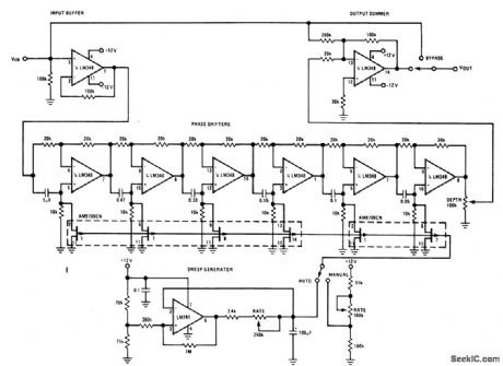
Sound-effect circuit sometimes called phase shifter simulates playing of two tape recorders having same material while varying speed of one by pressing on flange of tape reel. Resulting time delay causes some signals to be summed out of phase and canceled. Effect is that of rotating loudspeaker or of Doppler characteristic. Uses two LM348 quad opamps, two AM9709CN quad JFET devices, and one LM741 opamp. Phase-shift stages are spaced one octave apart from 160 to 3200 Hz in center of audio spectrum, with each stage providing 90' shift at its frequency. JFETs control phase shifters. Gate voltage of JFETs is adjusted from 5 V to 8 V either manually with foot-operated rheostat or automatically by LM741 triangle-wave generator whose rate is adjustable from 0.05 Hz to 5 Hz.- Audio Hand-book, National Semiconductor, Santa Clara, CA, 1977, p 5-10-5-11. (View)
View full Circuit Diagram | Comments | Reading(2173)
KEYED_FREE_RUNNING_MVBR
Published:2009/7/2 0:37:00 Author:May
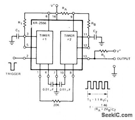
One section of Exar XR-2556 dual timer is operated in free-running mode, with other section used to provide ON/OFF keying. Frequency of oscillator is set by RA, RB, and C2. Timer 1 operates as mono MVBR with output connected to reset pin 8 of timer 2. Trigger drives pin 1 of timer 1 high, keying timer 2 on and producing tone-burst output for duration set by R1 and C1. Supply voltage is 4.5-16 V.- Timer Data Book, Exar Integrated Systems, Sunnyvale, CA, 1978, p 23-30. (View)
View full Circuit Diagram | Comments | Reading(1181)
EDGE_TRIGGERED_MONO
Published:2009/7/2 0:36:00 Author:May
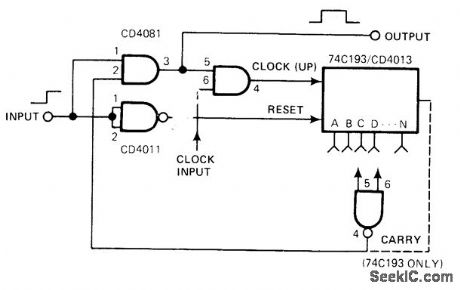
Output pulse width is precisely determined by external clock frequency and countdown factor N of 74C193 binary counter (t = N/f). Pulse is generated on rising edge of input, with output remaining high until count N is reached by binary counter. Counter resets and output returns instantly to zero if input pulse goes to zero before count of N. Value of N depends on which two counter outputs are connected to two-input NAND gate. With 74C193, 11 values of N between 1 and 16 are possible; with CD4013, values of N can range from t to 24,576.-R. L. Anderson, Digital One-Shot Produces Long, Accurate Pulses, EDN Magazine, March 5, 1978, p 127. (View)
View full Circuit Diagram | Comments | Reading(852)
LM3900_AS_MONO
Published:2009/7/2 0:35:00 Author:May
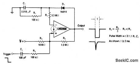
R4 holds output high normally, so C1 is charged almost to V+ level through D1. Negative input trigger forces output of current-differencing amplifier low, and C1 discharges through R1. When decreasing current through R2 approaches current in R3 (when voltage across C1 is about one-third of V+), output switches to high and returns circuit to standby state. Pulse width, equal to 1.1R1C1, can be programmed easily by using pot or some form of manual or electronic switching for R1 .-W. G. Jung, IC Op-Amp Cookbook, Howard W. Sams, Indianapolis, IN, 1974, p 510-512. (View)
View full Circuit Diagram | Comments | Reading(733)
PULSE_TRIGGERED_MONO
Published:2009/7/2 0:33:00 Author:May
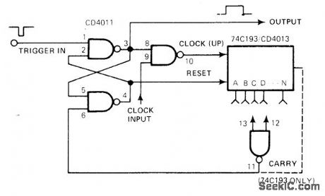
Combination of two ICs generates pulse having width precisely determined by external clock frequency and countdown factor N of 74C193 binary counter; time t in seconds is equal to N divided by frequency in hertz. With 74C193, 11 values of N are possible (1-6, 8-10, 12, and 16). With CD4013 14-stage counter, values of N can range from 1 to 24,576. Input pulse must be shorter than out-put pulse. Value of N depends on which two counter outputs are connected to two-input NAND gate.-R. L. Anderson, Digital One-Shot Produces Long, Accurate Pulses, EDN Magazine, March 5, 1978, p 127. (View)
View full Circuit Diagram | Comments | Reading(731)
1Hz_TO_10_MHz
Published:2009/7/2 0:32:00 Author:May
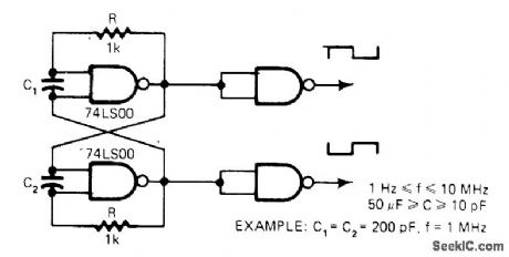
Simple circuit operating from single 5-V supply provides TTL output levels with reliable starting over wide frequency range. When capacitors are equal, period of oscillation is equal to 5×10³C s. By changing ratio of C1 to C2, duty cycle can be made as low as 20%.-D. B. Arnett, One-Chip TTL Oscillator Requires One 5V Supply, EDN Magazine, Jan. 5, 1978, p 96. (View)
View full Circuit Diagram | Comments | Reading(1048)
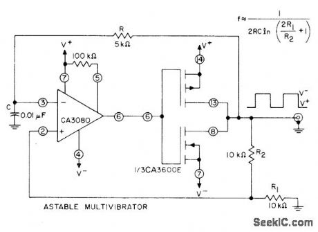
MONO_SQUARE_WAVE
Published:2009/7/2 0:30:00 Author:May
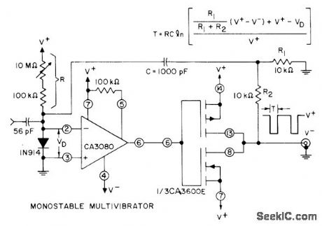
Stable characteristics of differential amplifier in CA3080 variable opamp assure pre be timing and threshold for output waveform. Opamp drives one inverter/amplifier section of CA3600E inverter array. Supply voltage range is ±3 to± 15V.- Circuit Ideas for RCA Linear ICs, RCA Solid State Division, Somerville, NJ, 1977, p 5. (View)
View full Circuit Diagram | Comments | Reading(602)
SQUARE_WAVE_BURSTS
Published:2009/7/2 0:29:00 Author:May
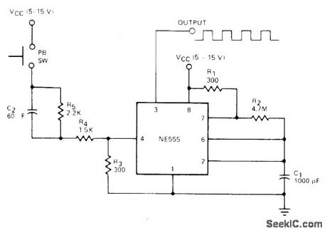
When pushbutton switch is closed, 555 timer generates square-wave tone bursts for duration depending on how long voltage on pin 4 exceeds threshold value. R1, R2, and C, control astable action of timer.- Signetics Analog Data Manual, Signetics, Sunnyvale, CA, 1977, p 726. (View)
View full Circuit Diagram | Comments | Reading(666)
ASYMMETRICAL_SQUARE_WAVES
Published:2009/7/2 0:28:00 Author:May
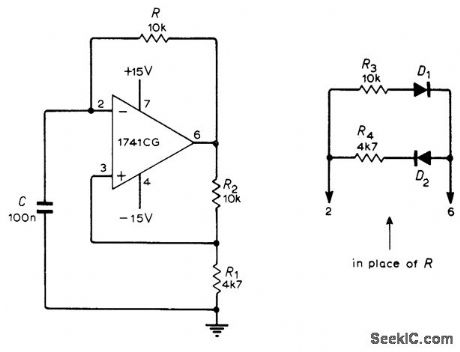
Addition of D1 and R4 to astable MVBR connection of 741 or equivalent opamp results in two different charging rates for C1, depending on whether opamp is in positive or negative saturation. Positive and negative peaks of output pulse then have different widths.-R. Melen and H. Garland, Understanding IC Operational Amplifiers, Howard W. Sams, Indianapolis, IN, 2nd Ed., 1978, p 122-123. (View)
View full Circuit Diagram | Comments | Reading(727)
FREE_RUNNING
Published:2009/7/2 0:27:00 Author:May
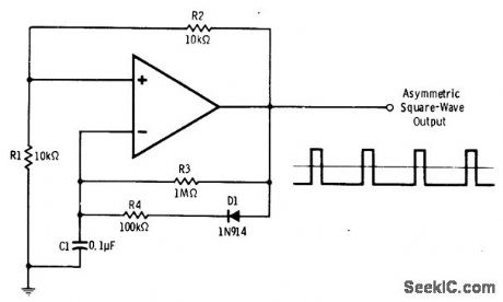
Positive feedback is applied to noninverting input terminal of oparnp through voltage divider R1-R2 to make amplifier switch regeneratively and repetitively between saturated states. Charging time of C controls duration of each state, to give desired free-running multivibrator providing rectangular (pin 6), trapezoidal (pin 3), and sawtooth (pin 2) sym-metrical waveforms. Article gives design equations and waveforms. For nonsymmetrical waveforms, use alternative circuit in place of R; here, diodes switch two different timing resistors into circuit alternately.-G. B. Clayton, Experiments with Operational Amplifiers, Wire-less World, May 1973, p 241-242. (View)
View full Circuit Diagram | Comments | Reading(765)
ASTABLE_SQUARE_WAVE
Published:2009/7/2 0:26:00 Author:May
CA3080 variable opamp drives one inverter/amplifier section of CA3600E inverter array. Quiescent power drain is typically 6 mW. Supply voltage range is ±3 to ±15V.- Circuit Ideas for RCA Linear ICs, RCA Solid State Division, Somerville, NJ, 1977, p 5. (View)
View full Circuit Diagram | Comments | Reading(637)
SEQUENTIAL_TIMING_GIVES_DELAYED_MONO_MVBR
Published:2009/7/2 0:25:00 Author:May
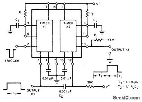
Output of first timer section of Exar XR-2556 dual timer is capacitively coupled to trigger pin of second timer section. When input trigger is applied, output 1 goes high for duration T1 = 1.1R1C1, then goes low and triggers timer 2 through CC. Output at pin 13 then goes high for duration T2 = 1.1R2C2 to give performance of delayed mono MVBR. Supply voltage is 4.5-16 V. Choose R, to keep timer output below 200 mA for supply voltage used.- Timer Data Book, Exar Integrated Systems, Sunnyvale, CA, 1978, p 23-30. (View)
View full Circuit Diagram | Comments | Reading(621)
455_Hz_ASTABLE
Published:2009/7/2 0:23:00 Author:May
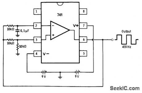
Frequency of square-wave output depends on values used for external capacitor and resistors. Very low frequencies can be obtained by using large values for both. High-frequency performance is limited by slew rate of opamp.-R. Melen and H. Garland, Understanding IC Operational Amplifiers, Howard W. Sams, Indianapolis, IN, 2nd Ed., 1978, p 119-120. (View)
View full Circuit Diagram | Comments | Reading(595)
HIGH_PRECISION_F_V_1
Published:2009/7/2 0:03:00 Author:May
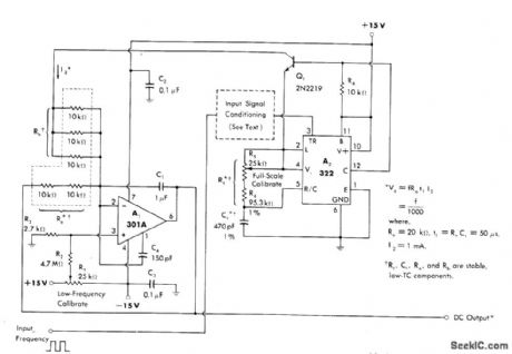
Components of V/F converter are reconnected to provide F/ V function.Inputfrequency up to 10 kHz is fed to 322 mono MVBR A2, either directly if pulsed or indirectly after conditioning. For low-frequency or slowly changing waveforms, zero crossing detector is used forinρut conditioning,A1isconnected asscaling amplifier and filter.-W. G .Jung, ''IC Timer Cookbook,″Howard W .Sams、lndianapoils,IN,1977,ρ 192-196. (View)
View full Circuit Diagram | Comments | Reading(600)
6_DIGIT_FOUR_FU_NCTION_1
Published:2009/7/1 23:54:00 Author:May
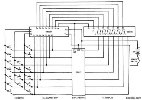
National MM5777 calculator chip requires only keyboard, NSA1161 LED display, DS8977 digit driver, and 9-V battery to provide add, subtract, multiply, and divide functions. Calculator chip includes keyboard encoding and key debouncing circuits, along with all clock and timing generators. LED segments can be driven directly, without multiplexing. Seventh digit position is used for negative sign of 6-digit number and as error indicator.Leading and trailing zero suppressionis included.-, MOS/LSI Databook, National Semiconductor,Santa Clara,GA,1977,p 8-84-8-89. (View)
View full Circuit Diagram | Comments | Reading(637)
6_DIGIT_FOUR_FU_NCTION
Published:2009/7/1 23:52:00 Author:May
National MM5777 calculator chip requires only keyboard, NSA1161 LED display, DS8977 digit driver, and 9-V battery to provide add, subtract, multiply, and divide functions. Calculator chip includes keyboard encoding and key debouncing circuits, along with all clock and timing generators. LED segments can be driven directly, without multiplexing. Seventh digit position is used for negative sign of 6-digit number and as error indicator.Leading and trailing zero suppressionis included.-, MOS/LSI Databook, National Semiconductor,Santa Clara,GA,1977,p 8-84-8-89. (View)
View full Circuit Diagram | Comments | Reading(804)
GIANT_NIXIE_SIGN
Published:2009/7/1 23:51:00 Author:May
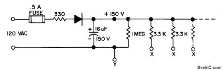
Simple power supply drives any desired number of alphameric Nixie characters each 21/2inches high to form illuminated house numbers, ON THE AIR sign for amateur station, or BAR IS CLOSED sign for party room. Connect 3.3K resistorfrom +150 V to pin 13 of each Nixie, and connect to point Y (-150 V) each segment to be lighted. Sign can be changed at any time by resoldering connections to segments.Diode must handle AC line voltage.-J.Grimes,Display Yourself in a Big Way,73 Magazine, Nov./Dec,1975,p 186-188. (View)
View full Circuit Diagram | Comments | Reading(626)
FIBEROPTIC_INTERFACE
Published:2009/7/1 23:47:00 Author:May
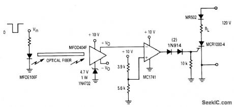
An op amp is used to interface between a fiberoptic system and the MOS SCR to multi-cycle,half-wave control of a load.This recelver has two complementary outputs,one at a quiescent level of about 0.6 V and the second at 3 V.By adding a 4.7 V zenerh senes with the return bus,the effective Vcc becomes 5.3V and also the 0.6V outputlevel is translated up to about 5.3 V.This level IS compatible with the reference input(5.9V) of the single-ended powered op-amp acting as a comparator. (View)
View full Circuit Diagram | Comments | Reading(763)
| Pages:295/471 At 20281282283284285286287288289290291292293294295296297298299300Under 20 |
Circuit Categories
power supply circuit
Amplifier Circuit
Basic Circuit
LED and Light Circuit
Sensor Circuit
Signal Processing
Electrical Equipment Circuit
Control Circuit
Remote Control Circuit
A/D-D/A Converter Circuit
Audio Circuit
Measuring and Test Circuit
Communication Circuit
Computer-Related Circuit
555 Circuit
Automotive Circuit
Repairing Circuit