
Basic Circuit
Index 296
CCD_DELAY_FOR_SPECIAL_EFFECTS
Published:2009/7/1 23:32:00 Author:May
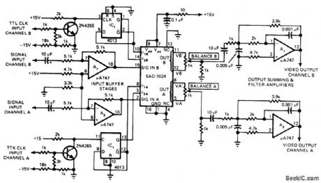
Basic bucket-brigade device incorporated in Reticon Corp. SAD-1024 charge-coupled-device delay line can synthesize such interesting audio-system delay effects as reverberation enhancement.chorus.and vibrato generation Other appIications include speech compression and voice scrambling Evaluation circuyt shown was developed by manulfacturer lnput clock frequencyis 200 kHz.and signal input is 5-kHz sine wave. Article describes operation of evaluation circuit in detail and presents variety of practical applications.-R. R. Buss. CCD's lmprove Audio System Performance and Generate Effects, EDN Magazine. Jan. 5. 1977. p55-61. (View)
View full Circuit Diagram | Comments | Reading(2720)
5_×_7_DOT_MATRIX
Published:2009/7/1 23:25:00 Author:May
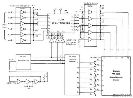
Drive for Dialight 745-0005 64-character alphamerle display generates desired character in response to pattern of 0s and 1s on input lines A1-A6. Timing of sequential scanning operation for seven horizontal rows of matrix is controlled by clock that drives binary counter having row-selecting outputs A, B, and C. Outputs C1-C5 of ROM correspond to vertical rows of dots enabled by 1-out-of-8 decoder.- Readout Displays, Dialight,Brooklyn, NY,1978,Catalog SG745,p 24-26. (View)
View full Circuit Diagram | Comments | Reading(988)
VOLTAGE_CONTROLLED_FILTER
Published:2009/7/1 23:22:00 Author:May
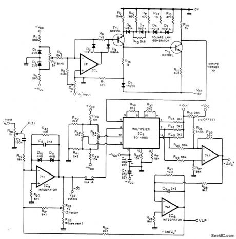
Used in elaborate sound synthesizer developed for generating wide variety of sounds. Serves as bandpass filter for which resonant frequency is Iinearly proportional to sum of input control voltages and a bias voltage. Can also be used as notch filter or as spectrum analyzer. Three-part articledescribes operation in detail and gives all other circuits of synthesizer. Supply voltages are 15 V.with polarity as indicated.-T. 0rr and D W. Thomas. Electronic sound Synthesizer、Wireless World. Part 2--Sept 1973.p 429-434(Part 1-Aug 1973.p366-372; Part 3-Oct.1973.p 485-490) (View)
View full Circuit Diagram | Comments | Reading(3327)
POSITIVE_INPUT_GIVES_RED
Published:2009/7/1 23:21:00 Author:May
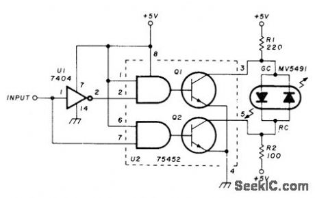
Uses Monsanto MV5491 dual LED having red and green light emitting diodes connected inversely in parallel,so current in onedirection gives green light and reverse current gives red. Circuit uses single SN75452 IC driver and one section of SN7404 hex inverter. High or positive input gives red indication, while low input gives green. Current limiting resistors R1 and R2 have different values because voltage and current specifications of parallel LEDs are different. Indicator appears to change color as input changes.-K. Powell,Novel Indicator Circuit, Ham Radio, April 1977,p 60-63. (View)
View full Circuit Diagram | Comments | Reading(1679)
ELECTRONIC_COMBINATION_LOCK
Published:2009/7/1 23:03:00 Author:May
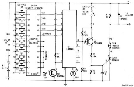


When button S12 (#) is pressed, a positive voltage fed through R1 appears at the base of transistor Q1, turning it on. When Q1 is conducting, pin 1 of U1 is brought to ground (low) or the battery's egative terminal. With pin 1 low, two things occur: Pin 8 of U1 goes high (+9 volts dc), turning on LED 1-indicating that the circuit has been armed-and pin 13 goes from high to low. Transistor Q2 requires a low signal or negative voltage on its base in order to conduct. It also needs a positive voltage on its emitter and a negative voltage on the collector. As long as the door switch (S15) remains open (with the door itself closed), Q2's emitter will not receive the necessary positive voltage. If, however, an unauthorized person opens the door, thus closing switch S15 and placing a positive voltage on the emitter of Q1, the following sequence occurs:
1. Transistor Q2 conducts, receiving the necessary biasing current through a currentdivider network consisting of resistors R3 and R4.2. As Q2 conducts, a voltage drop is developed across the voltage dividers made upof resistors R5 and R6. With R5 at 10,000 ohms and R6 at 1000 ohms, approximately one volt appears at the gate of SCR1. That's enough voltage to trigger the SCR's gate. (View)
View full Circuit Diagram | Comments | Reading(2277)
WIDE_RANGE_UJT_ORGAN
Published:2009/7/1 23:01:00 Author:May
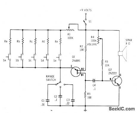
Combination of five individual resistor switches and three-ca-pacitor range switch gives 15 different audio frequencies for demonstration electronic organ oscillator feeding power amplifier and Ioud-speaker. R1 is adjusted for best combination of sounds. Any number of capacitors can be added. Battery drain is about 35 mA during operation. Pleasing tone sequence is obtained with resistor values of 6.8K. 8.2K. 10K. 12K. and 15K when range switch is set to 0.1,μF.-F. M.Mims. Electronic Music Projects.Vol. 1. Radio Shack. Fort Worth. TX. 1977. 2nd Ed. p 37-43. (View)
View full Circuit Diagram | Comments | Reading(839)
F_V_WITH_OUTPUT_FILTER_
Published:2009/7/1 23:01:00 Author:May
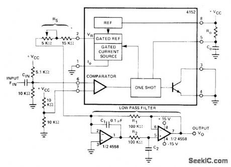
Two-pole low-pass active filter improves dynamic range and response time of Raytheon 4152 frequency-tovoltage converter. Ripple in output is less than 0.02 V P-P above 100 Hz. Requires ±15 V supply, Maximum inputfrequency is 10 kHzwhen CIN, is 0.002 μF, R0 is 6.8K, and C0 is 0.01μ F.- Linear Integrated Circuit Data Book, Raytheop Semiconductor Division, Mountain View, CA, 1978, p 7-48. (View)
View full Circuit Diagram | Comments | Reading(1093)
THREE_DIAL_COMBINATION_LOCk
Published:2009/7/1 22:56:00 Author:May
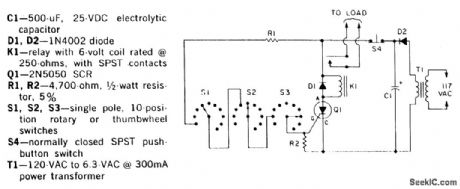
Here's an effective little combination lock that you can put together in one evening's time. To open the lock, simply dial in the correct combination on the three rotary or thumbwheel switches. With the correct combination entered, current flows through R1 into Q1's gate terminal, causing the SCR to latch in a conductive state. This sends a current through relay K1, which responds by closing its contacts and actuating whatever load is attached. After opening the lock, twirl the dials of S1 through S3 away from the correct combination so that nobody gets a look at it. The lock will remain open and your load will remain on because the SCR is latched on. To lock things up, it's only necessary to interrupt the flow of anode current through the SCR by pressing pushbutton S4. (View)
View full Circuit Diagram | Comments | Reading(991)
THREE_PART_HARMONY
Published:2009/7/1 22:54:00 Author:May

Four SC/MP microprocessors, one serving as conductor and three as instrumentalists, generate multiple parts for harmony feeding common loudspeaker system.Microprocessors have paralleled address and data buses, with 4K RAM connecting to lowest 4 bits of data bus Each microprocessor is supplied with list of notes by note number and notelengths as part of software,At end of each basicnote length.SC/MP1 checks each other processor to see if it is time to proceed to next notein list If h is.next note IS played by other processors untll signaled by conductor via memory Article glves software listing,-T Doone.Quar-tet of SC/MP's Plays Music for Trios EDN Magazine, Sept,20.1978.p57-58 and 60. (View)
View full Circuit Diagram | Comments | Reading(1086)
HIGH_OUTPUT_600_OHM_LINE_DRIVER
Published:2009/7/1 22:52:00 Author:May
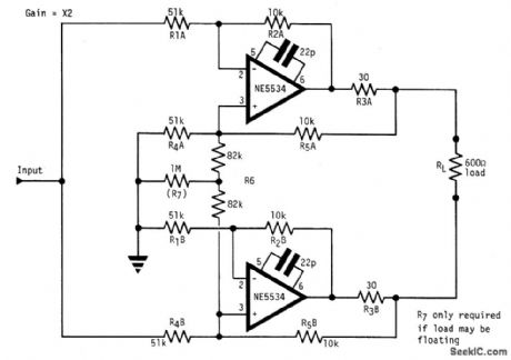
The circuit has a floating output, i.e., it behaves like an isolated transfonner winding, with the output amplitude remaining unchanged whether the center or either end of the load is grounded. This is achieved by making Z-out, common mode, infinite. The circuit consists of two current-sources in push-pull. Since each has infinite output Z, the common mode output impedance is also infinite. Connecting a resistor between the noninverting terminals of the op amps reduces the differential Z-out without affecting the Z-common-mode. Since the output is floating, if the load is also floating there is no output ground reference, which results in malfunction. This can be corrected by reducing the common-mode Z slightly. R7 fulfills this function. All resistors should be of close tolerance to give a good balance. The line driver provides +24 dB from ±12 V or + 16 dB from ±6 V supplies. (View)
View full Circuit Diagram | Comments | Reading(1062)
600_OHM_BALANCED_DRIVER_FOR_LINE_SIGNALS
Published:2009/7/1 22:48:00 Author:May
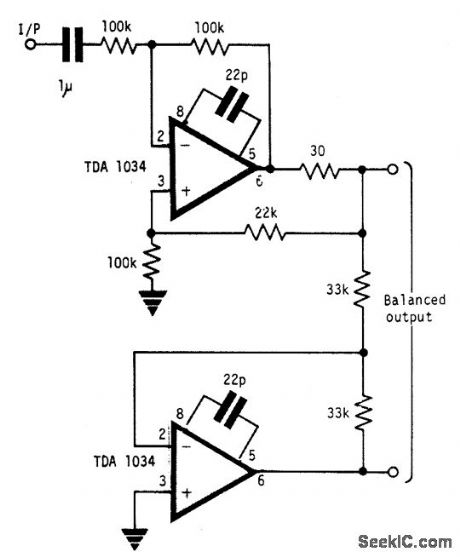
This circuit uses current and voltage feedback. This circuit will handle +24 dBm with ±12 volts supply using TDA 1034s. (View)
View full Circuit Diagram | Comments | Reading(989)
50_OHM_TRANSMISSION_LINE_DRIVER
Published:2009/7/1 22:46:00 Author:May
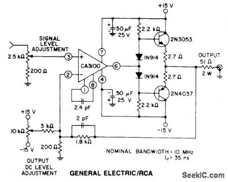
This circuit uses a wideband, high slew rate CA3100 BiMOS op amp. The slew rate for this amplifier is 28 V/μs. Output swing is 9 volts peak-to-peak into a terminated line, measured at the termination. (View)
View full Circuit Diagram | Comments | Reading(1625)
LED_WIND_VANE
Published:2009/7/1 22:44:00 Author:May
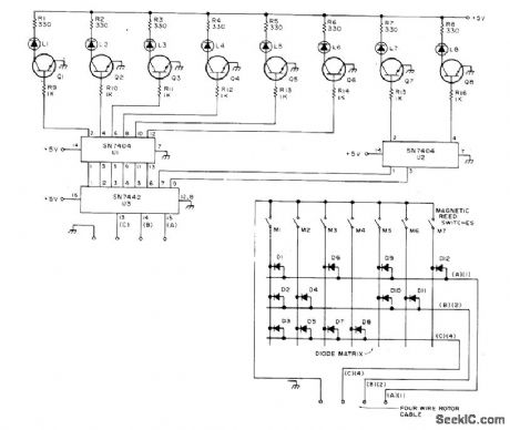
Ceramic magnet attached to rotor closes magnetic reed switches positioned at 45°intervals in circle around rotor. Eight wind directions are represented as 0-7 in binary notation,so 0= NW,1 = N,2 = NE,3=E,4=SE, 5 = S, 6 = SW, and 7 = W. Since 0 requires no switch, only seven switches are needed in rooftop indicator and only four wires need be run to binary decoder (wires A, B, C, and ground) driving LED readout in house. Transistors are 2N3641, and diodes in matrix used at vane location are 1N914 or 1N4148 silicon,-W. L.MacDowell, Digital Wind Direction Indicator, 73 Magazine, Nov. 1974, p 40-42. (View)
View full Circuit Diagram | Comments | Reading(2304)
FIVE_TRANSISTOR_AMPLIFIER_BOOSTS_FAST_PULSES_INTO_50_OHM_COAXIAL_CABLE
Published:2009/7/1 22:42:00 Author:May
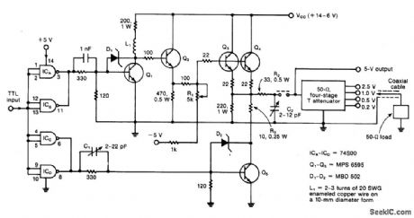
The circuit works from dc to 50 MHz and will deliver pulses as short as 10 ns. It is driven by a TTL signal through a 740S00 quad Schottky NAND gate, ICA through ICD. Transistor Ql,wired as a common-emitter amplifier, drives transistor Q2, a simple emitter follower. Transistors Q3 and Q4, wired in parallel, also form an emitter follower and drive the output. When Q3 and Q4 are both turned off, transistor Q5 works as a low-impedance sink. Schottky diodes D1 and D2 prevent Q1 and Q5 from becoming saturated. To adjust the circuit, potentiometer R1 is set to optimize the output pulse's fall time. Inductor L1, a peaking coil, should be adjusted to improve the rise time to within a permissible 5% overshoot. Likewise, capacitor C1 can be varied to control preshooting. Further output pulse shaping is accomplished with the help of capacitor C2.Resistors R2 and R3 ensure a proper 50-ohm impedance at the amplifier's output when the pulse is on or off, respectively. (View)
View full Circuit Diagram | Comments | Reading(991)
BINARY_DEMO
Published:2009/7/1 22:39:00 Author:May
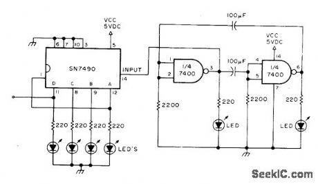
Two sections of SN7400 quad gate form low-frequency MVBR senring as pulse source for SN7490 decade counter. Rate is low enough so blinking of tED status indicators in MVBR can be seen, as indication of pulse generation. Similarly, LEDs of counter blink to indicate counts of 8, 4, 2, and n from left to fight, with combinations of lights coming on to display binary values 0 to 15 before recycling. Ideal for Science Fair exhibit.-A. MacLean, How Do You UselCs?, 73 Magazine, Dec, 1977,p 56-59. (View)
View full Circuit Diagram | Comments | Reading(2290)
5_DIGIT_FLUORESCENT_DIODES
Published:2009/7/1 22:37:00 Author:May
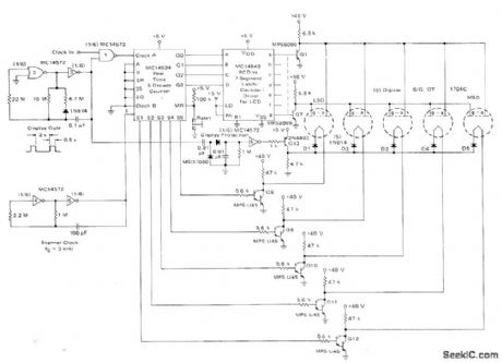
Realtime drive for five-decade counter requires only three lCs MC14534 contains five-decade ripple counter with output time multiplexed by internal scanner. Scanning rate is controlled by inverters 4 and 5 of MC14572. Multiplexed BCD outputs go to MC14543 7-segment decoder whose outputs drive fluorescent diodes.-A.Pshaenich, Interface Considerations for Numeric Display Systems, Motorola,Phoenix,AZ,1975,AN-741,p 10. (View)
View full Circuit Diagram | Comments | Reading(2273)
RAMP_FUNCTION
Published:2009/7/1 22:36:00 Author:May
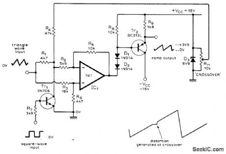
Circuit combines triangle and square-wave inputs from VCO in differen.tial amplifier having switched gain, to generate ramp function for use with variety of other waveforms in sound synthesizer designed for duplicating wide variety of sounds. Three-part article gives all circuits and operating details.-T. Orr and D. W, Thomas, Electronic Sound Syn thesizer, Wireless World, Part 1-Aug. 1973, p 366-372 (Part 2-Sept. 1973, p 429-434; Part 3-Oct.1976. p 485-490> (View)
View full Circuit Diagram | Comments | Reading(1320)
LINE_DRIVER_PROVIDES_FULL_RAIL_EXCURSIONS
Published:2009/7/1 22:33:00 Author:May
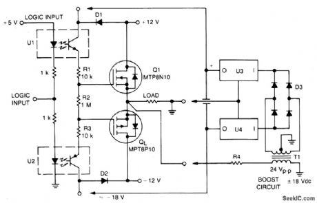
The login input is applied to opto-isolators U1 and U2 with, respectively, npn and PnP emitter follower outputs.Dc balance is adjusted by potentiometer R2. The emitter follower drive the gates of Q1 and Q2, the complementary TMOS pairs. With a±12V supply, the swing at the common source output point is about 12 V peak-to-peak.By adding a±18-V boost circuit, as shown, the output swing can approach the rail swing .This circuit applies the output to transformes T1 which is rectified by diode bridge D3,regulated by U3 and U4, and then applied to the collectors of U1 and U2. Diodes D1 and D2 are forward-biased when 12-V supplies are used, but they are back-biased when the 18-V boost is used (View)
View full Circuit Diagram | Comments | Reading(752)
REVERBERATION
Published:2009/7/1 22:30:00 Author:May
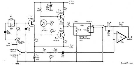
Used in sound synthesizer developed for generating wide variety of musical and other sounds. Four-transistor driver feeds spring-type reverberation unit at up to about 4 kHz, with switch giving choice of reverberation only or reverberation combined with input signal at VA. Amount of reverberation can be controlled manually with R3 or automatically with voltage-controlled amplifier or voltagecontrolled filter of synthesizer. Three-part article gives all circuits and describes operation in detaiL-T. 0rr and D. W. Thomas, Electronic Sound Synthesizer, Wireless World, Part 2-Sept. 1973, p 429-434 (Part 1-Aug. 1973, p 366-372; Part 3-Oct. 1973, p 485-490). (View)
View full Circuit Diagram | Comments | Reading(1335)
LED_BAR_GRAPH_DRIVER
Published:2009/7/1 22:18:00 Author:May
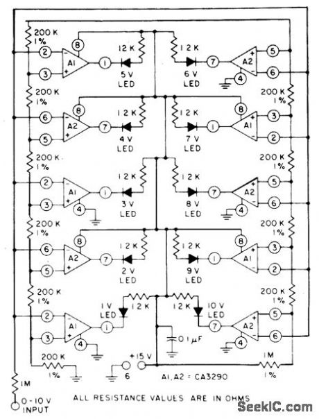
The circuit uses CA3290 BiMOS dual voltage comparators. Non-inverting inputs of A1and A2 are tied to voltage divider reference.The input signal is applied to the inverting inputs. LEDs are turned on wheninput voltage the reaches the voltage on the reference divider. (View)
View full Circuit Diagram | Comments | Reading(1074)
| Pages:296/471 At 20281282283284285286287288289290291292293294295296297298299300Under 20 |
Circuit Categories
power supply circuit
Amplifier Circuit
Basic Circuit
LED and Light Circuit
Sensor Circuit
Signal Processing
Electrical Equipment Circuit
Control Circuit
Remote Control Circuit
A/D-D/A Converter Circuit
Audio Circuit
Measuring and Test Circuit
Communication Circuit
Computer-Related Circuit
555 Circuit
Automotive Circuit
Repairing Circuit