
Circuit Diagram
Index 2155
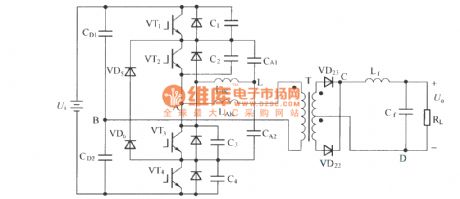
Main schematic circuit diagram of high-voltage power supply
Published:2011/3/24 21:26:00 Author:muriel | Keyword: Main schematic circuit diagram , high-voltage power supply
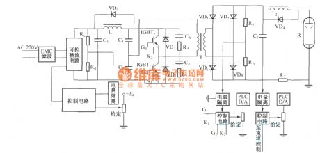
View full Circuit Diagram | Comments | Reading(808)
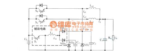
System chart of high-voltage power supply
Published:2011/3/24 21:29:00 Author:muriel | Keyword: System chart, high-voltage power supply
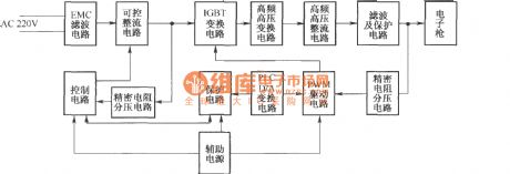
View full Circuit Diagram | Comments | Reading(596)
Modified phase shift full bridge ZVS main circuit
Published:2011/3/24 21:39:00 Author:muriel | Keyword: Modified phase shift full bridge ZVS main circuit

View full Circuit Diagram | Comments | Reading(873)
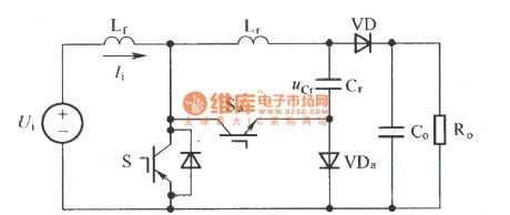
Modified full bridge phase shift ZVS-PWM DC/DC circuit
Published:2011/3/24 21:40:00 Author:muriel | Keyword: Modified, full bridge , phase shift , ZVS-PWM DC/DC circuit
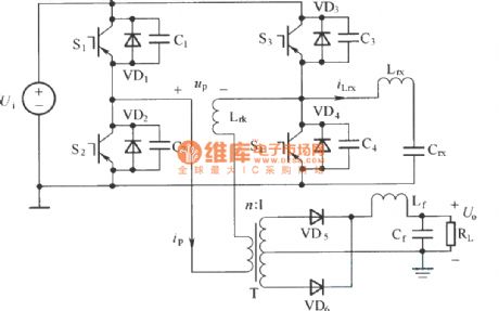
View full Circuit Diagram | Comments | Reading(1817)
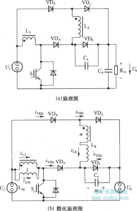
Modified ZVT-PWM converter topology
Published:2011/3/24 21:42:00 Author:muriel | Keyword: Modified, ZVT-PWM converter, topology
View full Circuit Diagram | Comments | Reading(606)
Modified ZCT-PWM converter topology
Published:2011/3/24 21:43:00 Author:muriel | Keyword: Modified ZCT-PWM converter topology
View full Circuit Diagram | Comments | Reading(560)
Flying capacitance clamped five level changing circuit
Published:2011/3/24 21:50:00 Author:muriel | Keyword: Flying capacitance clamped, five level, changing circuit

View full Circuit Diagram | Comments | Reading(487)
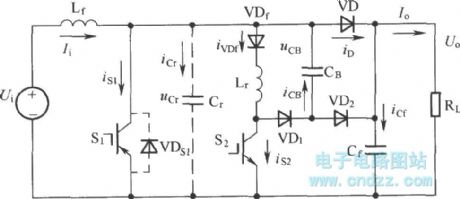
Passive lossless buffer circuit with minimum voltage stress
Published:2011/3/24 21:47:00 Author:muriel | Keyword: Passive , lossless, buffer circuit , minimum voltage stress
View full Circuit Diagram | Comments | Reading(548)
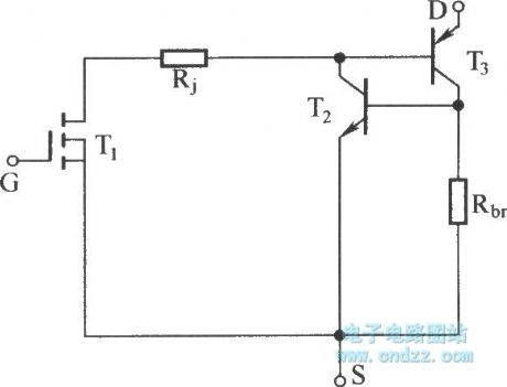
IGBT equivalent circuit with parasitic transistor
Published:2011/3/24 22:03:00 Author:muriel | Keyword: IGBT equivalent circuit, parasitic transistor
View full Circuit Diagram | Comments | Reading(916)
Short-circuit protection circuit with current sensor detection IGBT overcurrent
Published:2011/3/28 1:05:00 Author:muriel | Keyword: Short-circuit protection circuit, current sensor, IGBT overcurrent
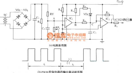
(a)electric schematic diagram
(b)PWM control circuit's output drive wave form (View)
View full Circuit Diagram | Comments | Reading(4096)
Wide load range no-voltage switch three level DC converter
Published:2011/3/28 1:01:00 Author:muriel | Keyword: Wide load range , no-voltage switch, three level, DC converter
View full Circuit Diagram | Comments | Reading(446)
Two-phase ZVT-PWM converter topology structure chart
Published:2011/3/24 22:35:00 Author:muriel | Keyword: Two-phase, ZVT-PWM , converter, topology structure chart
View full Circuit Diagram | Comments | Reading(499)
Two cells IGBT module of stray inductance
Published:2011/3/25 1:43:00 Author:muriel | Keyword: Two cells, IGBT module, stray inductance
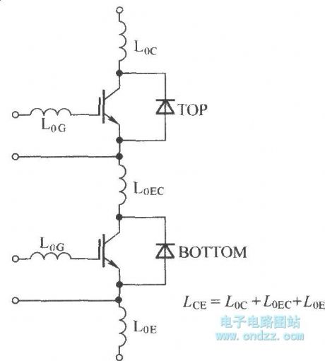
View full Circuit Diagram | Comments | Reading(1261)
Drive circuit (voltage-type)
Published:2011/3/24 22:24:00 Author:muriel | Keyword: Drive circuit , voltage-type
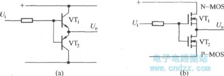
(a)as shown the drive circuit suitable for low frequency miniwatt drive, when the control signal Ui is high level, VT1 breakover, output voltage Uo corresponding control switch tube (IGBT) is breakover; When the control signal Ui is low level, VT2 breakover, output voltage Uo corresponding control switch tube (IGBT) be turn off.
(b) the drive circuit is shown by mosfet composition push-pull circuit, its working principle as figure (a) shows circuit. This circuit of high frequency peak value drive current can reach l0A above, it is suitable for high-power IGBT devices. (View)
View full Circuit Diagram | Comments | Reading(555)
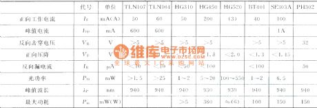
The main parameters of infrared light-emitting diode
Published:2011/4/7 1:50:00 Author:Rebekka | Keyword: infrared light-emitting diode
View full Circuit Diagram | Comments | Reading(625)
Relics anti-theft alarm circuit diagram
Published:2011/4/7 1:24:00 Author:Rebekka | Keyword: Relics anti-theft alarm
View full Circuit Diagram | Comments | Reading(773)
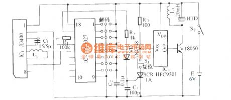
Detection code and transmission circuit diagram
Published:2011/4/7 1:19:00 Author:Rebekka | Keyword: Detection code and transmission
View full Circuit Diagram | Comments | Reading(744)
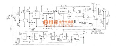
Radio reception and alarm circuit diagram
Published:2011/4/7 1:22:00 Author:Rebekka | Keyword: Radio reception and alarm
View full Circuit Diagram | Comments | Reading(560)
RS232 serial port circuit
Published:2011/3/22 3:12:00 Author:may | Keyword: serial port
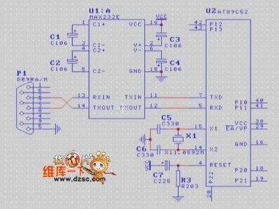
RS232 serial port circuit is shown in the following diagram:
(View)
View full Circuit Diagram | Comments | Reading(555)
drive lamp and relay laden simplify circuit diagram
Published:2011/3/25 1:46:00 Author:muriel | Keyword: drive lamp, relay laden , simplify circuit diagram
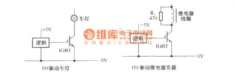
View full Circuit Diagram | Comments | Reading(435)
| Pages:2155/2234 At 2021412142214321442145214621472148214921502151215221532154215521562157215821592160Under 20 |
Circuit Categories
power supply circuit
Amplifier Circuit
Basic Circuit
LED and Light Circuit
Sensor Circuit
Signal Processing
Electrical Equipment Circuit
Control Circuit
Remote Control Circuit
A/D-D/A Converter Circuit
Audio Circuit
Measuring and Test Circuit
Communication Circuit
Computer-Related Circuit
555 Circuit
Automotive Circuit
Repairing Circuit