
Circuit Diagram
Index 75
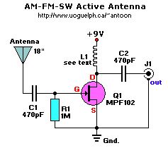
Active Antenna for AM/FM/SW 1
Published:2013/7/15 0:58:00 Author:muriel | Keyword: Active Antenna, AM/FM/SW
View full Circuit Diagram | Comments | Reading(1139)
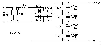
500 WATT PA 2
Published:2013/7/15 0:57:00 Author:muriel | Keyword: 500 WATT PA
View full Circuit Diagram | Comments | Reading(993)
500 WATT PA 1
Published:2013/7/15 0:57:00 Author:muriel | Keyword: 500 WATT PA
View full Circuit Diagram | Comments | Reading(1742)
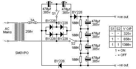
500 WATT PA
Published:2013/7/15 0:56:00 Author:muriel | Keyword: 500 WATT PA
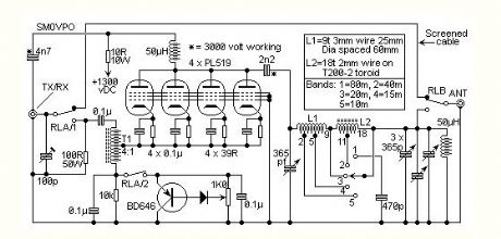
Although I am an avid proponent of QRP (using reasonable power levels), there are times when I wish that I could run 1,000,000 watts and point it in a particular direction. If you are reading this then you know exactly what I am writing about. Unfortunately, here in the real world, it is quite expensive to buy or build BIG linear amplifiers - until now.
This is the circuit of a 500 watt linear amplifier, based upon a design by Frits Geerligs, PA0FRI, who has his own homepage at http://home.planet.nl/~fhvgeerligs. The circuit uses four PL519 TV line output valves in a very simple circuit that will deliver over 450 watts at 3.5 MHz (350 watts at 30 MHz). PL519 (40KG6A) is a more robust replacement for the earlier PL509 (40KG6) tube. Both valves will work well in this circuit. The input drive power is about 50 - 100 watts so it is compatible with most amateur radio HF transmitters. Not shown in the circuit is the cooling fan that is required to force air around the valves to cool them. In operation the 1K0 pot is adjusted to set the total valve anode current to around 50mA to 70 mA.
T1 is a 4:1 balun wound on a 5cm ferrite rod. 9 + 9 turns. Connect the end of the first winding to the start of the second to form the center tap.
L1 is 9 turns of 3mm Dia wire, wound on a 25mm Dia, 60mm long former.
L2 is 18 turns on a toroidal former. Use two length of 2mm Dia wire, one with 11 turns and the other with 7 turns.
The 50 watt 100 ohm resistor recomended by PA0FRI is formed by two 50 ohm 25 watt non-inductive TO-220 resistors in series, bolted beside the fan. I use 100 x 10K carbon resistors aranged 10 x 10 between two pieces of 0.1 matrix wiring board (veroboard). My method is cheaper and avoids the need to mount input circuitry above chassis. All inputs are kept below the chassis whilst the valve anode terminals and output circuitry is kept below the chassis. The 100pf trimmer capacitor is adjusted for best VSWR from the driving transmitter at 29 MHz.
All four valve heaters (40 volts each) may be wired in series and connected to the 220 volt mains via a 6uf 250vAC capacitor for 50 Hz (5uf for 60 Hz). I personally favour the use of a 40 volt transformer winding, on a home-made transformer, to run all the valves heaters (in parallel) as well as the 40 volt fan. This places less strain on the cathode/heater insulation of old tubes that may have been kicked around in junk boxes for years.
PA0FRI sugests a power supply circuit which is switcheable and delivers 325 volts, 650 volts or 1300 volts to the amplifier. The circuit is very clever, and shown below for your interest.
(View)
View full Circuit Diagram | Comments | Reading(1616)
QRP HF LINEAR AMPLIFIER
Published:2013/7/15 0:55:00 Author:muriel | Keyword: QRP , HF , LINEAR AMPLIFIER
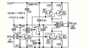
This project was a particular surprise for me in that the BC547 (equiv 2N2222) can be used to build a 500mW linear amplifer covering the entire HF band with excelent spectral purity and no neutralising at all. Ugly-bug construction was used but I dare say that the good results are partly to do with the method of construction.
The circuit is fairly straight-forward and does not even need any form of RF neutralising. Two pairs of BC547 transistors are used in a push-pull type of output stage, biassed by a single diode and resistor. The driver is also very conventional using T1 to transform the drive impedance to a very low value for the output pairs. The amplifier is constructed on a piece of copper-clad board 45mm long by 17mm wide. Superglue a 44mm long by 3mm wide strip of copper-clad board along the center. This will become the battery supply rail. Using a sharp knife, remove some copper to form a 3mm x 3mm pad at one end of the battery rail to form the RF output terminal. Next fit the 10n and 33n decoupling capacitors; one pair at either end. These should lay flat on the board. The rest is easy after you see the photographs.
T1 primary is 14-turns of very thin wire (0.1mm Dia.) and the secondary is 1+1 turn of thin wire (0.2mm Dia.). T1 former is two of the smallest ferrite beads I could find. You can just see it in the left-hand photograph above. T1 is composed of two grey ferrite beads. The right-hand photograph shows T2 and the mounting of the two output pairs of BC547 transistors.
T2 is a little special. I found two small ferrite rings in the junk-box and decided to give them a try. The windings are 11-turns triflar wound using thin wire (0.2mm Dia.):
Twist together three 1-metre lengths of thin enamelled wire.
Wind 11-turns through the ferrite rings (1-turn is passed through both rings). Do NOT cut off the surplus yet.
Identify A1-A2, B1-B2, C1-C2 using an ohm-meter.
Thread each end of C1 and C2 back through the ferrite rings to add 2-1/2 extra turns to each end. Winding C should now have a total of 16-turns.
Twist together A2 and B1 and connect to the positive battery rail.
Connect A1 and B2 to the BC547 collectors.
The five transistors are all mounted on their heads using super-glue and with their legs in the air spread wide apart (Hey! this sounds kinda' pornographic!!). The finished linear amplifer does not look very pretty but it is very small. It is less than 10mm high and looks like this. Here you can see it beside my parker pen for comparison (I thought it would be better than a common 1-crown coin).
(View)
View full Circuit Diagram | Comments | Reading(1627)
5-Watt Transmitter
Published:2013/7/15 0:54:00 Author:muriel | Keyword: 5-Watt Transmitter
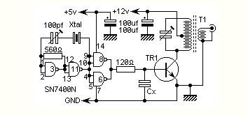
This is a very simple 5 watt CW TX based upon a TTL logic chip. There is just one tricky component and this is Cx. This component should have an impedance of about 10 - 50 ohms at the frequency of interest. If you wish to reduce the transmitter power, increase the value of Cx. It is Cx which causes the square wave from the output transistor to approximate a sine waveform. The value of Cx is the price of simplicity in this TX.
STARTING values for Cx are as follows (but there is a LOT of leeway)
1.8 MHz = 4.7nf
3.5 MHz = 2.2nf
7.0 MHz = 1.2nf
10 MHz = 820pf
14 MHz = 560pf
18 MHz = 470pf
24 MHz = 390pf
28 MHz = 330pf
It is far better to use too high a value for Cx initially then reduce it to achieve the correct RF output power. The value of Cx will depend upon your choice of TR1. Virtually any RF power transistor will work well in this application, as long as it will handle 800mA continuously. I have even used a BC108 in this application but the RF power was restricted to about 150mW. Cx was about 5x the value quoted above.
The output tuned circuit uses a coil WITHOUT ferrite slug. Use the usual rule-of-thumb formula for the tuned circuit;
Coil = Wavelength (in meters) = number of turns
Capacitor = Wavelength (in meters) = Capacitance (pf)
This will get you in the right area although it could differ widely with different coil formers. The coil output winding is from 5% to 15% of the total number of turns. Adjust the output winding before reducing the value of Cx. You need the least number of turns that will give you the power needed.
Connect +5 volts to the SN7400 chip and +12 volts to the PA and you will have over five watts of power out. To key the TX put the key in the +12v lead.
You MUST use an antenna LP-filter with this rig if you are using a good antenna. If the antenna is tuned (magnetic loop or frame antennas etc) then you need not bother with the LP-filter. Do NOT use a linear amplifier for this transmitter. The finished transmitter will fit into a matchbox with a little care.
I have received a comment from one constructor that if a 5-ohm resistor is fitted in the emitter of the transistor two things happen; 1. the output power increases, 2. It draws less current.
(View)
View full Circuit Diagram | Comments | Reading(0)
HF BANDS QRP LINEAR AMPLIFIER
Published:2013/7/15 0:51:00 Author:muriel | Keyword: HF BANDS , QRP , LINEAR AMPLIFIER

This is a rather unusual QRP Power Amplifier design, with a wide frequency response; within three dB's from 300KHz to 30MHz. Overall gain is in the region of 16dB and the final output power may be well over four watts.
The wide bandwidth is a result of the construction of the RF transformers, T1 and T2. These are wound on 2-hole ferrite balun cores as commonly found in the old fashioned valve TV sets (e.g. Phillips 4322-020-31520). Twist 2 lengths of 22 SWG enamelled wire together and wind as shown. Connect the end of the A winding to the start of the B winding. Use this junction as the centre-tap of the transformer.
This PA will deliver 4 watts continuously (with a suitable heatsink), and may be loaded into a short-circuit or open circuit without causing damage. This makes it almost the ideal PA for outdoor/field use. Above is the full circuit diagram of the RFPA and the coil winding pattern. This PA may be used for for SSB, as well as CW (and AM?).
Set RV1 to MINIMUM resistance and apply 12volt power with NO DRIVE. Adjust RV1 for about 250mA DC total supply current. This may be be reduced to a much smaller current if lower output powers (reduced drive) is used.
(View)
View full Circuit Diagram | Comments | Reading(1088)
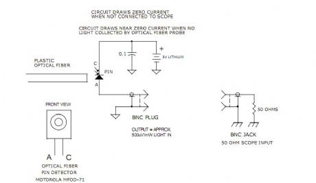
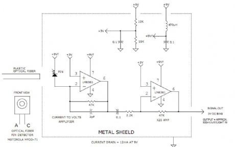
BROAD BAND 50MHz OPTICAL FIBER RECEIVER
Published:2013/7/15 0:46:00 Author:muriel | Keyword: BROAD BAND , 50MHz , OPTICAL, FIBER RECEIVER
View full Circuit Diagram | Comments | Reading(841)
BROAD BAND 2MHz OPTICAL FIBER RECEIVERS
Published:2013/7/15 0:44:00 Author:muriel | Keyword: BROAD BAND , 2MHz, OPTICAL FIBER RECEIVERS
View full Circuit Diagram | Comments | Reading(813)
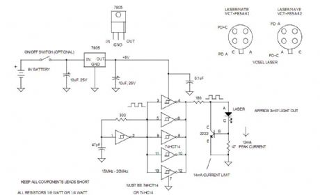
20MHz VCSEL 3mW LASER TEST CIRCUITS
Published:2013/7/15 0:43:00 Author:muriel | Keyword: 20MHz, VCSEL, 3mW , LASER TEST CIRCUITS
View full Circuit Diagram | Comments | Reading(1474)
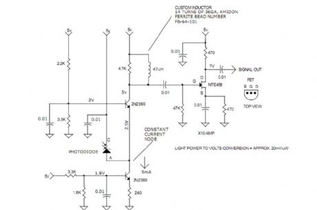
10MHz TO 20MHz LASER LIGHT DETECTORS
Published:2013/7/15 0:42:00 Author:muriel | Keyword: 10MHz TO 20MHz, LASER LIGHT, DETECTORS
View full Circuit Diagram | Comments | Reading(1290)
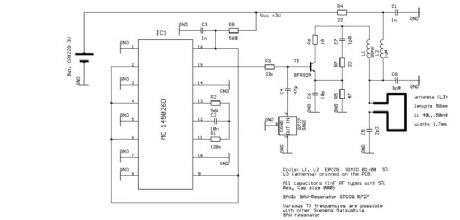
Remote-control transmitter for 433.92 MHz
Published:2013/7/11 22:40:00 Author:muriel | Keyword: Remote-control transmitter, 433.92 MHz
View full Circuit Diagram | Comments | Reading(4764)
Pierce oscillator
Published:2013/7/11 22:39:00 Author:muriel | Keyword: Pierce oscillator
View full Circuit Diagram | Comments | Reading(3350)
Colpitts oscillator with common base
Published:2013/7/11 22:39:00 Author:muriel | Keyword: Colpitts oscillator, common base
View full Circuit Diagram | Comments | Reading(2252)
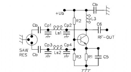
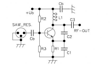
SAWR-based transmitters
Published:2013/7/11 22:38:00 Author:muriel | Keyword: SAWR-based transmitters
View full Circuit Diagram | Comments | Reading(863)
SAW-based transmitter design appnote from RFM 2
Published:2013/7/11 22:37:00 Author:muriel | Keyword: SAW-based transmitter
View full Circuit Diagram | Comments | Reading(1371)
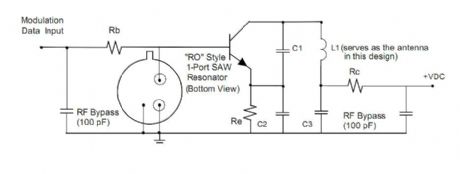
SAW-based transmitter design appnote from RFM
Published:2013/7/11 22:37:00 Author:muriel | Keyword: SAW-based transmitter
View full Circuit Diagram | Comments | Reading(1587)
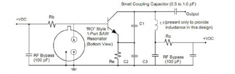
SAW-based 434MHz transmitter schematic with RO2101 (from appnote below)
Published:2013/7/11 22:36:00 Author:muriel | Keyword: SAW-based , 434MHz, transmitter schematic, RO2101

View full Circuit Diagram | Comments | Reading(3518)
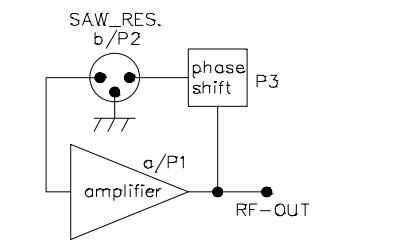
SP-Elektroniikka superregenerative receiver and SAW-based transmitter
Published:2013/7/11 22:35:00 Author:muriel | Keyword: SP-Elektroniikka, superregenerative, receiver , SAW-based transmitter
View full Circuit Diagram | Comments | Reading(903)
434MHz short-range communications 2
Published:2013/7/11 22:35:00 Author:muriel | Keyword: 434MHz , short-range communications
View full Circuit Diagram | Comments | Reading(1315)
| Pages:75/2234 At 206162636465666768697071727374757677787980Under 20 |
Circuit Categories
power supply circuit
Amplifier Circuit
Basic Circuit
LED and Light Circuit
Sensor Circuit
Signal Processing
Electrical Equipment Circuit
Control Circuit
Remote Control Circuit
A/D-D/A Converter Circuit
Audio Circuit
Measuring and Test Circuit
Communication Circuit
Computer-Related Circuit
555 Circuit
Automotive Circuit
Repairing Circuit