
Circuit Diagram
Index 882
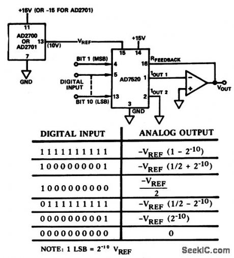
8_bit_D_A_convertor_with_digitally_controlled_set_point
Published:2009/7/20 3:57:00 Author:Jessie
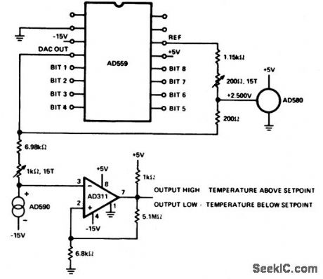
8-bit D/A convertor with digitally controlled set point(courtesy Analog Devices, Inc.). (View)
View full Circuit Diagram | Comments | Reading(1145)
LOW_BATTERY_DETECTOR
Published:2009/7/9 20:55:00 Author:May
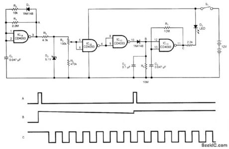
The battery low-voltage detector uses a CD4093 Schmitt trigger and a capacitor that acts as a 1-bit dynamic RAM. The circuit conserves power by using a periodic test method. IC1A, C1, R1, R2, and D1 generate a narrow, positive pulse at point A.
D2, R4, and R5 regulate and divide the signal at A. Thus, the input of IC1B is independent of the power supply. Because the threshold voltage of the Schmitt trigger depends on the power supply, the threshold voltage will drop if the power-supply voltage drops. When the threshold voltage is lower than the input voltage, IC1B will become low, and IC1C's output will become high.
Capacitor C2 stores the results of the periodic test. The time constant C2 and R6 set is 1 s, and the test period is approximately 0.1 s. When point B is high, which implies that the battery is low, IC1D, C3, and R7 generate a square waveform, which lights D3. You can adjust the detected voltage level by adjusting R4. You can test different battery voltages by changing the voltage level of D2. (View)
View full Circuit Diagram | Comments | Reading(0)
33_watt_AF_power_amplifier_using_an_ECG1118
Published:2009/7/20 3:56:00 Author:Jessie
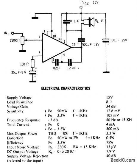
3.3-watt AF power amplifier using an ECG1118. This circuit is intended for phonograph applications (courtesy GTE Sylvania Incorporated). (View)
View full Circuit Diagram | Comments | Reading(656)
Temperature_to_frequency_convener_using_a_Datel_VFQ_1_14_pin_DIP_
Published:2009/7/20 3:56:00 Author:Jessie
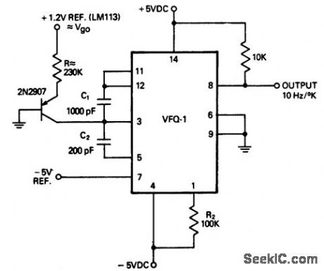
Temperature-to-frequency convener using a Datel VFQ-1 14-pin DIP (courtesy Datel Systems, Inc.). (View)
View full Circuit Diagram | Comments | Reading(975)
D_A_converter_with_10_volt_reference
Published:2009/7/20 3:55:00 Author:Jessie
D/A converter with 10-volt reference (courtesy Analog Dodoes, Inc.). (View)
View full Circuit Diagram | Comments | Reading(928)
STABILIZED_LOW_INPUT_CAPACITANCE_BUFFER
Published:2009/7/9 20:53:00 Author:May
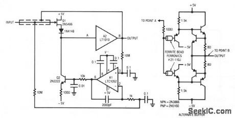
Q1 and Q2 constitute a simple, high-speed FET input buffer. Q1 functions as a source follower, with the Q2 current source load setting the drain-source channel current. The LT1010 buffer provides output drive capability for cables or whatever load is required. Normally, this open-loop configuration would be quite drifty because there is no dc feedback. The LTC1052 contributes this function to stabilize the circuit.It does this by comparing the filtered circuit output to a similarly filtered version of the input signal. The amplified difference between these signals is used to set Q2's bias, and hence Q1's channel current. Q1's source line ensures that the gate never forward biases, and the 2000 pF capacitor at A1 provides stable loop compensation. The rc network in A1's output prevents it from seeing high-speed edges coupled through Q2's collector-base junction. A2's output is also fed back to the shield around Q1's gate lead, bootstrapping the circuit's effective input capacitance down to less than 1 pF. (View)
View full Circuit Diagram | Comments | Reading(873)
2_watt_AF_power_amplifier_for_a_16_ohm_load
Published:2009/7/20 3:54:00 Author:Jessie
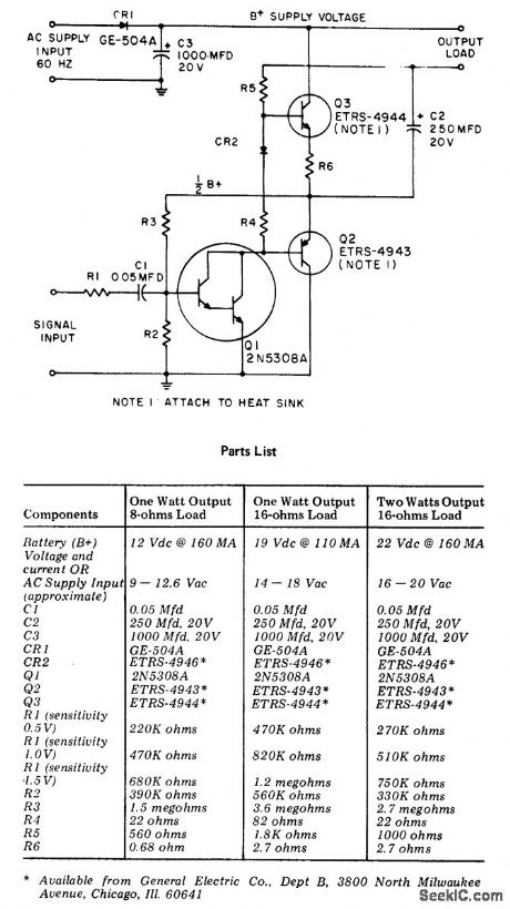
2-watt AF power amplifier for a 16-ohm load (courtesy General Electric Company). (View)
View full Circuit Diagram | Comments | Reading(719)
10_bit_D_A_converter_connected_for_two_quadrant_multiplication_
Published:2009/7/20 3:54:00 Author:Jessie
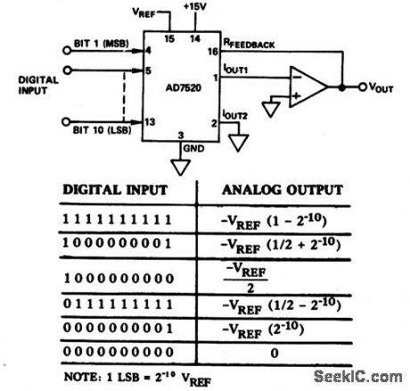
10-bit D/A converter connected for two-quadrant multiplication (courtesy Analog Devices, Inc.). (View)
View full Circuit Diagram | Comments | Reading(838)
IR_TRANSMITTER
Published:2009/7/9 20:53:00 Author:May
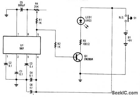
Using an NE567 as a tone oscillator, this circuit produces an IR signal from the LED, which is modu-lated with a square wave. LED1 is an IR-emitting LED. The modulation helps improve performance under high ambient light conditions. (View)
View full Circuit Diagram | Comments | Reading(0)
A_D_converter
Published:2009/7/20 3:54:00 Author:Jessie
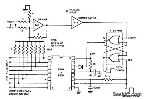
A/D converter.The circuit shown is an 8-bit binary A/D converter when using the 8240 or a 2-digit BCD A/D converter when using the 8250.The input strobe first resets then triggers the 8240/8250 and set the flip-flop,which enables the counter. The stair case from the op amp counts down until reaches the analog input, at which time the comparator resets the flip-flop and stops the count,The digital word at the eight outputs is the complementary binary or BCD equivalent of the analog input.As shown the maximum conversion time is 2.6 ms,determined by R and c at pin 14 of the counter.The not-Q output of the flip-flop is convenient to use as a data ready flag since it is high when conversion is complete(courtesy Intersil, Inc.). (View)
View full Circuit Diagram | Comments | Reading(0)
RELAY_OUTPUT_PROXIMITY_SENSOR
Published:2009/7/9 20:53:00 Author:May
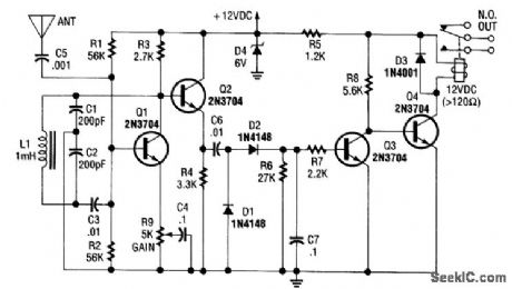
Q1 is used as an oscillator around 300 kHz. R9 is set so that the oscillator just begins to run. An object near the antenna will load the circuit down, and stop the oscillations. This is detected by bufferQ2,diodes D1 and D2, and this activates relay driver Q4, which operates the relay. (View)
View full Circuit Diagram | Comments | Reading(2409)
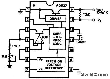
Celsius_temperature_to_frequency_converter
Published:2009/7/20 3:52:00 Author:Jessie
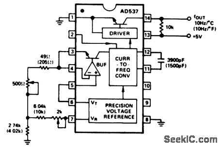
Celsius (Fahrenheit) temperature-to-frequency converter. No sensor is required since the AD537 has an internal VTEMP output. The converter output tracks the temperature at a rate of 10 hertz per degree Celsius or Fahrenheit, depending on the resistor-capacitor values chosen. All values in parentheses are for Fahrenheit. To calibrate measure the room temperature in Kelvin. Measure the temperature output at pin 6 at that temperature. Calculate the offset adjustment by dividing the VTEMP at pin 6 in milli volts by the room temperature in Kelvin, then multiplying by 273.2 The offset voltage will be in milli volts. Then disconnect the 49-ohm resistor and adjust the 2K pot for the offset voltage at pin 7. Connect the 49dm resistor. Then adjust the 500-ohm slope trimmer for room temperature, or 25℃, which results in 250 hertz (courtesy Analog Devices, Inc.). (View)
View full Circuit Diagram | Comments | Reading(1060)
Complete_cassette_record_playback_circuit_using_an_ECG1110_16_pin_DIP_that_provides_2_watts_of_audio_power
Published:2009/7/20 3:52:00 Author:Jessie
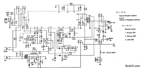
Complete cassette record/playback circuit using an ECG1110 16-pin DIP that provides 2 watts of audio power. This IC includes a preamplifier, tone amplifier and power amplifier. The 2-watt rating is or an 8-ohm load. Recommended supply voltage is 9volts. Typical voltage gains for each section are as follows: preamplifier, 60 dB; tone amplifier, 60 dB; and power amplifier, 40 dB (courtesy GTE Sylvania Incorporated). (View)
View full Circuit Diagram | Comments | Reading(711)
DIGITALLY_SELECTABLE_INPUTS_AND_GAIN
Published:2009/7/9 20:52:00 Author:May
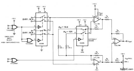
Low-power DG306 and DG305 analog switehes provide choice of 10.4 or 101 gain and choice of two differential input channels for instrumentation applications. Highest gain is obtained when control logic is high.- Analog Switches and Their Applications,''siliconix,Santa Clara,CA,1976,p 7-91. (View)
View full Circuit Diagram | Comments | Reading(888)
Digital_4_to_20_mA_or_1_to_5_volt_converter_
Published:2009/7/20 3:51:00 Author:Jessie
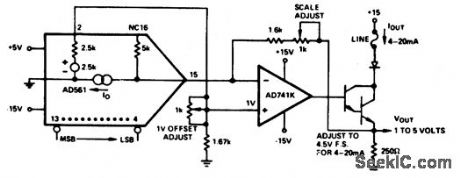
Digital 4-to-20 mA or 1-to-5 volt converter (courtesy Analog Devices, Inc.). (View)
View full Circuit Diagram | Comments | Reading(878)
BATTERY_SAVING_DISCONNECT_SWITCH
Published:2009/7/9 20:52:00 Author:May
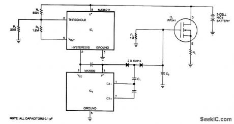
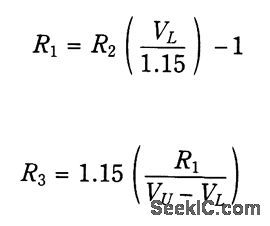


At a predetermined level of declining terminal voltage, the circuit disconnects the battery from the load and halts potentially destructive battery discharge. Q1, a high-side, floating-source MOSFET, acts as the switch. The overall circuit draws about 500 μA when the switch is closed and about 8 μA when it's open.
The values of Ry, R2, and R3 set the upper and lower voltage thresholds, Vu and Vy,, according to the relationships
For the circuit to start,V+ must exceed Vu. The voltage detector IC1 then powers IC2, but only while V+ remains above VL. Otherwise, IC2 loses its power, removes gate drive from Q1, and turns it off. IC2 is a dual charge-pump inverter that normally converts 5 V to ±10 V. Capacitors C1, C2, and the two associated diodes form a voltage tripler that generates a gate drive for Q1 that is approximately equal to two times the battery voltage.
With the values in the schematic, the circuit disconnects 3-cell Nicad battery from its load when V+ reaches a VL of 3,1 V. Approximately 0.5 V of hysteresis prevents the switch from turning on immediately when the circuit removes the load; V+ must first return to Vu, which is 3.6 V. The gate drive declines as the battery voltage declines, cause the ON-resistance of Q1 to reach a maximum of approximately 0.1 Ω, just before Y+ reaches its 3.1-V threshold. A 300-mA load current at that time will cause a 30-mV drop across the disconnect switch, The drop will be 2 to 3 mV less for higher battery voltages. Resistor R4 ensures that Q1 can adequately turn off by providing a discharge path for C2. (View)
View full Circuit Diagram | Comments | Reading(1290)
Fast_precision_10_bit_A_D_converter
Published:2009/7/20 3:50:00 Author:Jessie
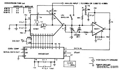
Fast precision 10-bit A/D converter (courtesy Analog Devices, Inc.). (View)
View full Circuit Diagram | Comments | Reading(868)
Kelvin_temperature_to_frequency_converter
Published:2009/7/20 3:49:00 Author:Jessie
Kelvin temperature-to-frequency converter. No sensor is required since the AD537 has an internal VTEMP output,The output tracks the temperature at 10 hertz per degree kelvin.To calibrate, select a 25℃ standard,which corresponds to 298°K, and adjust the 2K pot for 2.98 kHz(courtesy Analog Devices, Inc.). (View)
View full Circuit Diagram | Comments | Reading(977)
SIMPLE_IR_TRANSMITTER
Published:2009/7/9 20:50:00 Author:May
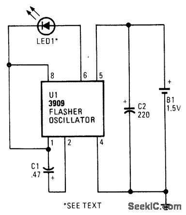
The IR diode's flash rate is determined by the value of C1, a 220-μF capacitor that sets the rate of oscillation at 1 Hz per second. Reducing C1 will increase the frequency of the circuit, while larger values will decrease the frequency.
Because the circuit only sends out single, nar-row pulses of invisible light, the IR receiver only responds with a click for every output pulse. (View)
View full Circuit Diagram | Comments | Reading(1039)
Successive_approximation_A_D_converter
Published:2009/7/20 3:48:00 Author:Jessie
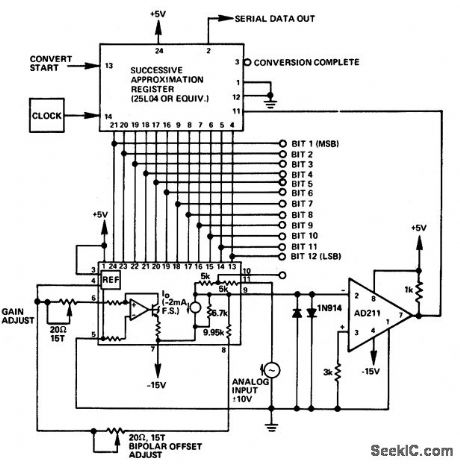
Successive approximation A/D converter (courtesy Analog Devices, Inc.). (View)
View full Circuit Diagram | Comments | Reading(1882)
| Pages:882/2234 At 20881882883884885886887888889890891892893894895896897898899900Under 20 |
Circuit Categories
power supply circuit
Amplifier Circuit
Basic Circuit
LED and Light Circuit
Sensor Circuit
Signal Processing
Electrical Equipment Circuit
Control Circuit
Remote Control Circuit
A/D-D/A Converter Circuit
Audio Circuit
Measuring and Test Circuit
Communication Circuit
Computer-Related Circuit
555 Circuit
Automotive Circuit
Repairing Circuit