
Measuring and Test Circuit
Index 57
SMOKE_GAS_VAPOR_DETECTOR
Published:2009/7/7 7:07:00 Author:May
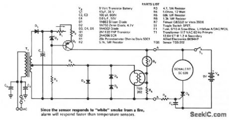
Transformer T1 supplies power to the heater of the sensor. Since the sensor is fairly sensitive to heater voltage, diodes D3, D4, and D5 regulate the heater voltage. T1, together with D1 and C2, forms a dc power supply, whose current is regulated by Q1 and adjusted by R1. The constant current from Q1 feeds a variable resistance, consisting of thermistor R7 and the parallel combination of R5 and the sensor resistance. When a hazard causes the voltage at A-A to drop, the net voltage at the SCR gate turns posi-tive, triggering the SCR on and operating the alarm. The alarm draws a small amount of current, so the battery will last a long time. Switch S1 turns off the alarm and resets the SCR. (View)
View full Circuit Diagram | Comments | Reading(854)
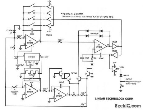
METHANE_CONCENTRATION_DETECTOR_WITH_LINEARIZED_OUTPUT
Published:2009/7/7 7:05:00 Author:May
View full Circuit Diagram | Comments | Reading(941)
SMOKE_DETECTOR
Published:2009/7/7 7:03:00 Author:May
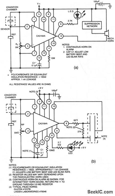
Use CA3164A BiMOS detector/alarm system. For operation as smoke detector with electromechan-ical horn (Fig. 40-1a), the output of driver at terminal8 is used. Large npn transistor Q3, with an active pull-up and transistor Q2 provide over 300 mA of drive current. For operation as a smoke detector with a piezoelectric ham (Fig. 40-1b), the circuit requires output from a second inverting amplifier at terminal 10, as well as the output from terminal 8. (View)
View full Circuit Diagram | Comments | Reading(0)
VARIABLE_DUTY_CYCLE_TIMER
Published:2009/7/7 6:46:00 Author:May
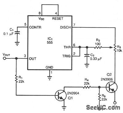
When configured as a free-running multivibra-tor, a 555 timer provides no more than a 50% duty cycle. By adding two transistors, however, you can obtain a variable 5 to 95% duty cycle without changing the sum of the on and off times. WhenVOUT decreases, Q1 is on and Q2 is off, disconnect-ing V+ while timing capacitor C2 discharges into pin 7 of the timer. When VOUT increases, Q2 reconnects V+ for recharging C2.Adjusting linear trimming potentiometer R3 to increase the charging resistance increases the on time, but decreases the off time by the same amount by lowering the discharge resistance (the converse is also true). As a result, the sum of the on and off times remains constant. R2 protects Q2 and the timer against high-charge/discharge currents. (View)
View full Circuit Diagram | Comments | Reading(2268)
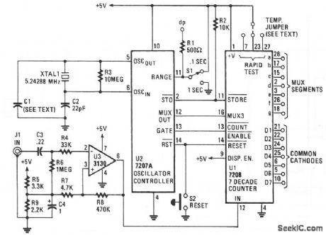
12_GHz_FREQUENCY_COUNTER
Published:2009/7/7 6:38:00 Author:May
The output of the CA3179 is fed through the D1/Q1 circuit. Those components serve to boost the 1-V output of the CA3179 to a standard TTL level. Then, depending on the position of range switch S2b, the signal is passed directly to the 7216, or through the divide-by-four circuit built from the two D flip-flops in IC3.
The other half of the range switch S2a controls the voltage at pin 3 of the CA3179. When pin 3 is high, the signal applied to pin 9 is fed through an extra internal divide-by-four stage before it is amplified and output on pins 4 and 5. When pin 3 is low, the signal on pin 13 is simply processed for output without being divided internally.
A 3.90625-MHz crystal provides the time base; the crystal yields a fast gate time of 0.256 second.The displayed frequency equals the input frequency divided by 1000 in the fast mode. In slow mode, gate time is 2.56 seconds. The displayed frequency equals the input frequency divided by 100 in the slow mode.
Switch S4, gate time, performs two functions. First it selects the appropriate gate time according to which digit output of IC1 the range input is connected to. Another of the 7216's inputs is also contro0ed by S4: the dp select input. The decimal point of the digit output to which that pin is connected will be the one that lights up. The correct decimal point illuminates, according to the position of S4, to provide a reading in MHz.
(View)
View full Circuit Diagram | Comments | Reading(2000)
40_MHz_UNIVERSAL_COUNTER
Published:2009/7/7 6:21:00 Author:May
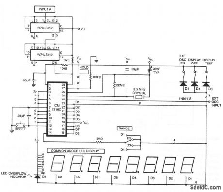
This circuit can be used to measure frequencies up to 40 MHz. To obtain the correct measured value, it is necessary to divide the oscillator frequency and the input frequency by four. In doing this, the time between measurements is also lengthened to 800 ms and the display multiplex rate is decreased to 125 Hz.
(View)
View full Circuit Diagram | Comments | Reading(1949)
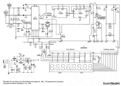
10_MHz_FREQUENCY_COUNTER
Published:2009/7/7 6:17:00 Author:May
The circuit consists of ICM7208 seven-decade counter U1, ICM7207A oscillator controller U2, and CA3130 biFET op amp U3. IC UI counts input signals, decodes them to 7-segment format, and outputs signals that are used to drive a 7-digit display. IC U2 provides the timing for U1, while U3 conditions the input to U1. The The circuit consists of ICM7208 seven-decade counter U1, ICM7207A oscillator controller U2, and CA3130 biFET op amp U3. IC U1counts input signals, decodes them to 7-segment format, and outputs signals that are used to drive a 7-digit display. IC U2 provides the timing for U1, while U3 conditions the input to U1. The 5.24288-MHz crystal frequency is divided by U2 to produce a 1280-MHz multiplexing signal at pin 12 of U2. That signal is input to U1 at pin 16 and used to scan the display digits in sequence.crystal frequency is divided by U2 to produce a 1280-MHz multiplexing signal at pin 12 of U2. That signal is input to U1 at pin 16 and used to scan the display digits in sequence. (View)
View full Circuit Diagram | Comments | Reading(0)
LOW_COST_FREQUENCT_COUNTER
Published:2009/7/7 5:54:00 Author:May
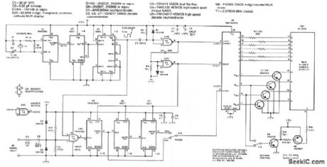
This counter uses a four-digit display, but with a flip of the range switch, it can display frequencies from 1 to 40 MHz, with a resolution of 100 Hz. The MM74C926 CMOS IC contains a four-digit decimal counter that can latch a given count and then use this information to drive a 7-segment, common-cathode multiplexed (MUX) display. The block diagram and schematic show the operation of the counter. Crystal-controlled timer U1 through U3 produces a 5-Hz square wave used for timing the frequency count. Y1 is a TV color-burst crystal operating in a reliable circuit that controls the oscillator frequency. U1 acts as the oscillator and also divides the fundamental operating frequency of 3.579545 MHz to produce a square-wave output of 60 Hz. U2 divides the 60-Hz output of U1 by six. In turn, the 10-Hz output of U2 is divided by two in U3, a dual flip-flop, to produce the 5-Hz pulse.
A quad, two-input, Schmitt-triggered NAND U4 is used for gating the rf-signal input and for generating the counter control pulses-Section U4D is unused. The 5-Hz output pulse of U3 is applied to the rf-signal input gate at U4A pin 2. When the timer output signal is low, the gate is closed. (View)
View full Circuit Diagram | Comments | Reading(3937)
PULSE_HEIGHT_TO_WIDTH_CONVERTER
Published:2009/7/7 5:37:00 Author:May
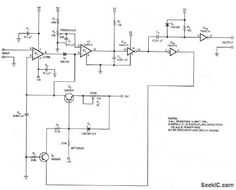
The output-pulse width from the circuit is a linear function of the input pulse's height. You can set the circuit's input threshold to discriminate against low-level pulses, while fixed components limit the circuit's maximum output-pulse width.
With a 270-KΩ resistor connected from the -9 V supply to the base lead of Q2, this circuit can handle input pulses separated by 20 μs for correct operation. The turn-off time of zener diode D2 sets the lower limit for the input-pulse repetition rate.
IC1, D1, and C3 detect the peak of the input pulse. The comparator IC2, triggers at your preset threshold. The RC delay network, R9 and C5, hold off inverter IC3's changing state until the completion of peak detection. After IC3A changes state, Q1 turns on and then turns on Q2, a constant-current source.
Constant-current source Q1 then discharges C3, the peak-detecting capacitor. When C3 has discharged below IC2's threshold, IC2's output decreases, as do pins 6 and 4 of IC3. The output-pulse width is a function of this discharge time, which you can adjust with R6. C6 and R7 control the maximum output-pulse width, which is 8 μs max. (View)
View full Circuit Diagram | Comments | Reading(0)
SQUARE_TO_SINE_WAVE_CONVERTER
Published:2009/7/7 5:29:00 Author:May
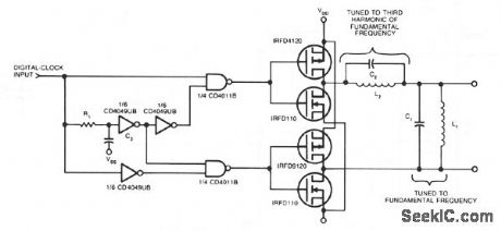
Two pairs of MOSFETs form a bridge that alternately switches current in opposite directions. Two parallel-resonant LC circuits complete the converter. The L1/C1 combination is resonant at the fundamental frequency; the L2/C2 combination is resonant at the clock frequency's third harmonic and acts as a trap. T1 and C3 ensure that both halves of the MOSFET bridge are never on at the same time by providing a common delay to the gate drive of each half. Select the values of R1 and C3 to yield a time constant that's less than 5% of the clock's period. You can add an output amplifter for additional buffering and conditioning of the circuit's sine-wave output. (View)
View full Circuit Diagram | Comments | Reading(2314)
10W_ON_2_METERS
Published:2009/7/7 5:29:00 Author:May
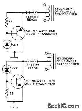
Linear power amplifierfor 2-meter transverter delivers 10 W PEP using two Siliconix VMP1 Mospower FETs. L1 and L2 are 8 turns, and L3 and L4 are 5 turns, all close-wound with No. 20 enamelon 3-mm form. Tran-sistor requires heatsink, insulated from chassis with 0.062-in beryllium oxide insulators. Effi-ciency is about 40%. -L. Leighton, Two-Meter Transverter Using Power FETs, Ham Radio, Sept. 1976, p 10-15. (View)
View full Circuit Diagram | Comments | Reading(840)
EIGHT_CHANNEL_TELEMETER
Published:2009/7/7 5:11:00 Author:May
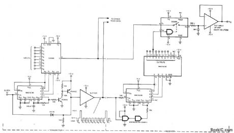
Multiplex transmission system permits monitoring eight different inputs at remote location, 5-V pulse train is sent down separate channel to receiving location to perform timing and synchronizing functions for outputs of MM74C42 BCD-to-decimal decoder. 15-V reset pulse is superimposed on 5-V clock. Other receivers can be added if monitoring is desired at more than one location.- Analog Switches and Their Applications, Siliconix, Santa Clara, CA, 1976, p 7-71-7-72. (View)
View full Circuit Diagram | Comments | Reading(1047)
ADJUSTABLE_AC_TIMER.2_TO_10_SEC
Published:2009/7/7 5:01:00 Author:May
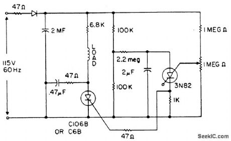
View full Circuit Diagram | Comments | Reading(675)
LOW_POWER_MICROPROCESSOR_PROGRAMMABLE_INTERVAL_TIMER
Published:2009/7/7 4:58:00 Author:May
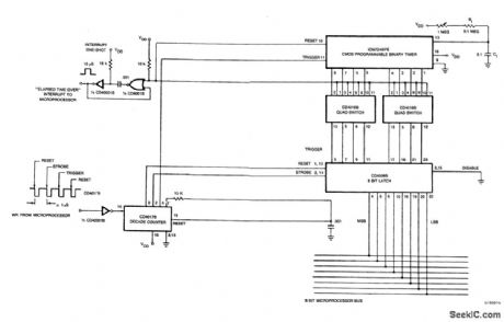
The microprocessor sends out an 8-bit binary code on its 8-bit I/O bus (the binary value needed to program the ICM7240), followed by four WRITE pulses into the CD4017B decade counter. The first pulse resets the 8-bit latch, the second strobes the binary value into the 8-bit latch, the third triggers the ICM7240 to begin its timing cycle and the fourth resets the decade counter. The ICM7240 then counts the interval of time determined by the R-C value on pin 13, and the programmed binary count on pins 1 through 8. At the end of the programmed time interval, the interrupt one-shot is triggered, informing the microprocessor that the programmed time interval is over. With a resistor of approximately 10 M ohm and a can capacitor of 0.1,ttF, the time base of the ICM7240 is one second. Thus, a time of 1-255 seconds can be programmed by the microprocessor, and by varying R or C, longer or shorter time bases can be selected. (View)
View full Circuit Diagram | Comments | Reading(1334)
BUCK_BOOST_CONVERTER
Published:2009/7/7 4:32:00 Author:May

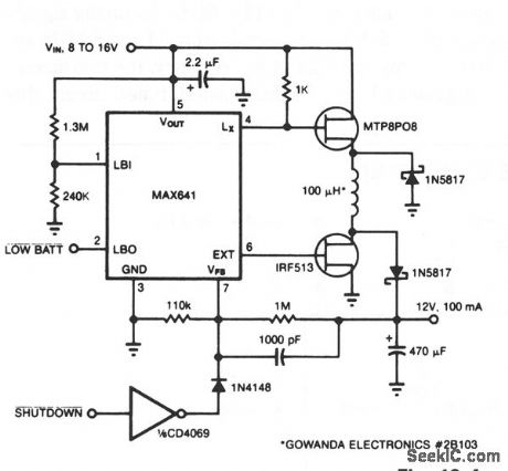
This converter can accommodate wide input-voltage swtngs,such as the 8 to 15-V swing typicalof a 12-V sealed lead/acid battery.The low batteryoutput indicates when mput voltage drops below 8V. Pulling shutdown turns off the circuit. (View)
View full Circuit Diagram | Comments | Reading(1211)
PROGRAMMABLE_VOLTAGE_CONTROLLED_TIMER
Published:2009/7/7 4:31:00 Author:May
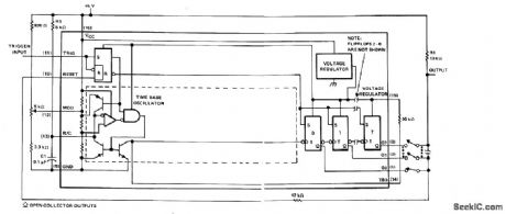
The μA2240 may easily be configured as a programmable voltage controlled timer with a minimum number of external components. The modulation input (pin 12), which allows external adjustment of the input threshold level. A variable voltage is applied from the arm of a 10 k ohm potentiometer connected from VCC to ground. A change in the modulation input voltage will result in a change in the time base oscillator frequency and the period of the time base output (TBO). The TBO has an open-collector output that is connected to the regulator output via a 10 k ohm pull-up resistor. The output of the TBO drives the input to the 8-stage counter section.At start-up, a positive trigger pulse starts the TBO and sets all counter outputs to a low state. The binary outputs are open-collector stages that may be connected together to the 10 k ohm pull-up resistor to provide a wired-OR output function. This circuit may be used to generate 255 discrete time delays that are integer multiples of the time-base period. The total delay is the sum of the number of time-base periods, which is the binary sum of the Q outputs connected. Delays from 200 μs to 0.223 s are possible with this configuration. (View)
View full Circuit Diagram | Comments | Reading(860)
PHASE_SEQUENCE_DETECTOR
Published:2009/7/7 4:28:00 Author:May
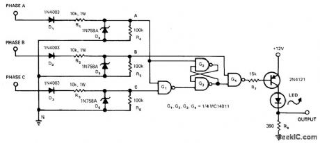

Circuit detects incorrect phase sequence of motor driving pump, compressor, conveyor, or other quipment that can be damaged by reverse rotation.Circuit also protects motor from phase loss that could cause rapid temperature rise and heat damage. LED is on when phasing is correct. For phase loss or incorrect sequence, output goes low and LED is dark. Diodes and zeners change sine waves for all phases to rectangular logiclevel pulses that feed gates. When phases are correct, output of G4 is train of rectangular pulses about 2.5 ns wide. Output is zero for incorrect sequences. Since leading edge of output pulse coincides with positive zero crossing of phase B, output pulses can be used to trigger SCR connected across phase B and driving relay-coil load. SCR then energizes relay only when sequence is correct.-H. Normet, Detector Protects 3.Phase-Powered Equipment, EDN Magazine, Aug. 5, 1978, p 78 and 80. (View)
View full Circuit Diagram | Comments | Reading(0)
PHASE_REVERSAL_DETECTOR
Published:2009/7/7 4:22:00 Author:May
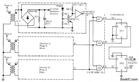
Used in three-phase applications in which direction of rotation of phases is critical, as in three-phase motors where reversal of two phases can provide disastrous reversal of motor. Line voltages are stepped down and isolated by control-type transformers, Each phase is half-wave rectified and shaped by 1N4001 diode and MPS5172 transistor, with additional shaping by MC14572 inverter. Shaped outputs of all three phases are combined in AND gates G1-G3 to give pulse out-puts sequentially. D flip-flops are connected to sense change in sequence of pulses caused by reversal of one or more input phases. Flip-flop output can be used to trip relay or other protective device for removing air conditioner or other equipment from line before it is damaged.-T. Malarkey, A Simple Line Phase-Reversal Detection Circuit, Motorola, Phoenix, AZ, 1975, EB-54. (View)
View full Circuit Diagram | Comments | Reading(2626)
LOGIC_LINE_MONITOR
Published:2009/7/7 3:57:00 Author:May
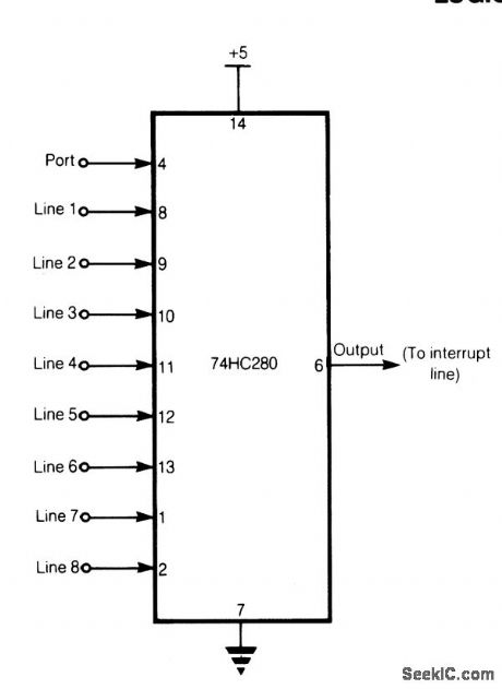
This circuit requires only one CMOS IC, which is available in a 14-pin surface-mount package. The figure shows the logic lines going to a standard 9-bit parity comparator chip. This device is conventionally used in data transmission and recording applications to provide a means of error-detection by comparing the received eight- or nine-bit words with their corresponding parity bits. If the sum of the one's in a received word is odd but the odd-par-ity bit is low, then that word is known to be in error and requires retransmission.
When one of the logic lines decreases, the output of the parity comparator decreases, generating a wake-up interrupt to the microprocessor. The ninth line comes from a port on the microprocessor and is toggled to reset the output signal high again, ready for the next logic change.
(View)
View full Circuit Diagram | Comments | Reading(874)
XOR_GATE_UP_DOWN_COUNTER
Published:2009/7/7 3:24:00 Author:May
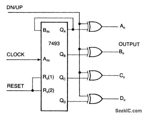
One can transform an ordinary binary counter, such as a 7493, into an up/down counter with mode control by adding XOR gates 7486 to the counter's outputs. The circuit counts up when the DN/UP line is low and down when the DN/UP line is high.
To use the 7493 counter to count out its maximum count length of 0 - 15, connect the QA output to the BIN input and apply clock pulses to the AIN input. The reset input, when high, inhibits the count inputs and simultaneously retums the outputs AO through DO to low in the up-count mode or 15 in the down-count mode. For normal counting, the reset input must be low. 0ne can easily cascade this counter by feeding the QD line to the clock input of a succeeding counter.
(View)
View full Circuit Diagram | Comments | Reading(3823)
| Pages:57/101 At 204142434445464748495051525354555657585960Under 20 |
Circuit Categories
power supply circuit
Amplifier Circuit
Basic Circuit
LED and Light Circuit
Sensor Circuit
Signal Processing
Electrical Equipment Circuit
Control Circuit
Remote Control Circuit
A/D-D/A Converter Circuit
Audio Circuit
Measuring and Test Circuit
Communication Circuit
Computer-Related Circuit
555 Circuit
Automotive Circuit
Repairing Circuit