
Oscillator Circuit
Index 41
10_MHz_OSCILLATOR
Published:2009/6/29 4:36:00 Author:May
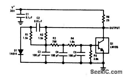
View full Circuit Diagram | Comments | Reading(770)
400_MHz_OSCILLATOR_
Published:2009/6/29 4:35:00 Author:May
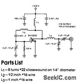
View full Circuit Diagram | Comments | Reading(821)
LOW_DISTORTION_OSCILLATOR
Published:2009/6/29 4:34:00 Author:May
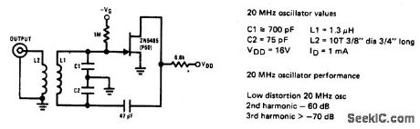
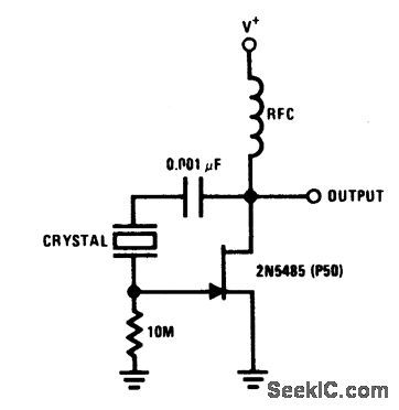
The 2N5485 JFET is capable of oscillating in a circuit where harmonic distortion is very low. The JFET local oscillator is excellent when a low harmonic content is required for a good mixer circuit. (View)
View full Circuit Diagram | Comments | Reading(0)
500_MHz_OSCILLATOR
Published:2009/6/29 4:33:00 Author:May
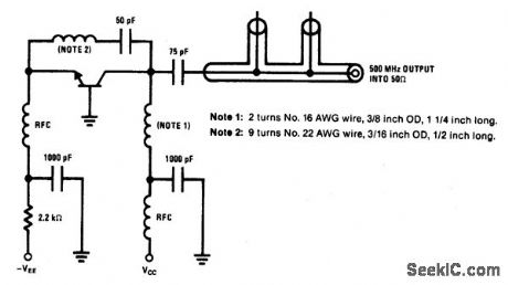
View full Circuit Diagram | Comments | Reading(736)
SUPPRESSING_OSCILLATION
Published:2009/6/28 23:36:00 Author:May
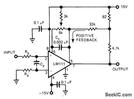
Use of positive feedback to pin 5 of comparatorgives sharp and clean output transitions even with slow triangle-wave inputs, with no possibility of comparator bursting into oscillation near crossing point. Input resistors should not be wirewound.Circuit will handle triangle-wave inputs up to several hundred kilohertz.—P. Lefferts, Overcome Comparator Oscillation Through Use of Careful Design, EDN Magazine, May20, 1978, p 123-124. (View)
View full Circuit Diagram | Comments | Reading(752)
74 Series digital circuit of 74LS324 VCO (dual-phase output with controlling)
Published:2011/8/1 20:11:00 Author:Lucas | Keyword: 74 Series, digital circuit , VCO, dual-phase output , controlling)
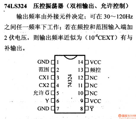
Output frequency is determined by the external components; it can works in the frequency of 30 ~ 120Hz; if the input is added 2V voltage in the frequency controlling range, the output frequency is approximately 0.0001CEXT , and there is complementary out.
(View)
View full Circuit Diagram | Comments | Reading(1197)
74 Series digital circuit of 74LS3237 dual voltage-controlled oscillator(single-phase output)
Published:2011/8/1 1:25:00 Author:Lucas | Keyword: 74 Series , digital circuit , dual voltage-controlled oscillator, single-phase output

Two independent voltage-controlled oscillators; external components can determine the output frequency; it works in any frequency between 0.12 and 30MHz.
(View)
View full Circuit Diagram | Comments | Reading(733)
TRANSMITTER_OSCILLOSCOPE_COUPLER_FOR_CB_SIGNALS
Published:2009/6/26 2:24:00 Author:May
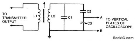
To display an rf signal, connect L1 to the transmitter and points A and B to the vertical plates of the oscilloscope. Adjust L1 for minimum SWR and C3 for the desired trace height on the CRT. L2 = 4 turns #18 on 3/4 slug tuned rf coil form, L1 = 3 turns #22 adjacent to grounded end of L1, C1, and C2 = 5 pF, C3 = 75 pF trimmer. (View)
View full Circuit Diagram | Comments | Reading(713)
OSCILLOSCOPE_CONVERTER_PROVIDES_FOUR_CHANNEL_DISPLAYS
Published:2009/6/26 2:17:00 Author:May
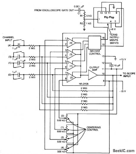
The monolithic quad operational amplifier provides an inexpensive way to increase display capability of a standard oscilloscope. Binary inputs drive the IC op amp; a dual flip-flop divides the scope's gate output to obtain channel selection signals. All channels have cen-tering controls for nulling offset voltage. AL negative-going scope gate signal selects the next channel after each trace. The circuit operates out to 5 MHz. (View)
View full Circuit Diagram | Comments | Reading(948)
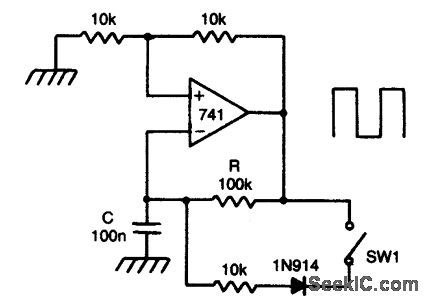
ASTABLE_OSCILLATOR
Published:2009/6/26 1:59:00 Author:May
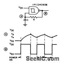
Before power is applied, the input and output are at ground potential and capacitor C is discharged. On power-on, the output goes high (VDD) and C charges through R until Vis reached. the output then goes low (VSS). C is now discharged through R until Vn is reached.The output then goes high and charges C towards Vp through R. Thus input A alternately swings between Vp and Vn as the output goes high and low. This circuit is self-starting at power-on. (View)
View full Circuit Diagram | Comments | Reading(901)
CMOS_OSCILLATOR
Published:2009/6/25 21:34:00 Author:May
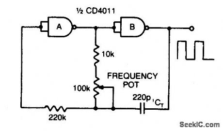
Varying the 100 K pot changes the discharge rate of CT and hence the frequency. A square wave output is generated. The maximum frequency using CMOS is limited to 2 MHz. (View)
View full Circuit Diagram | Comments | Reading(150)
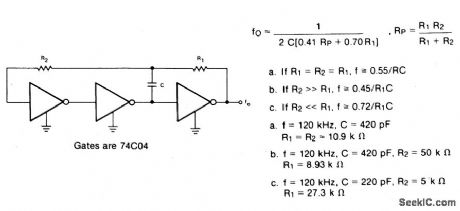
SQUARE_WAVE_OSCILLATOR
Published:2009/6/25 21:24:00 Author:May
View full Circuit Diagram | Comments | Reading(0)
1_kHz_SQUARE_WAVE_OSCILLATOR
Published:2009/6/25 21:22:00 Author:May
View full Circuit Diagram | Comments | Reading(0)
R_C_OSCILLATOR
Published:2009/6/25 21:21:00 Author:May
View full Circuit Diagram | Comments | Reading(0)
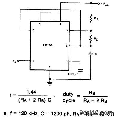
555_TIMER_OSCILLATOR
Published:2009/6/25 4:46:00 Author:May
View full Circuit Diagram | Comments | Reading(989)
FREE_RUNNING_OSCILLATOR_
Published:2009/6/25 4:44:00 Author:May
View full Circuit Diagram | Comments | Reading(780)
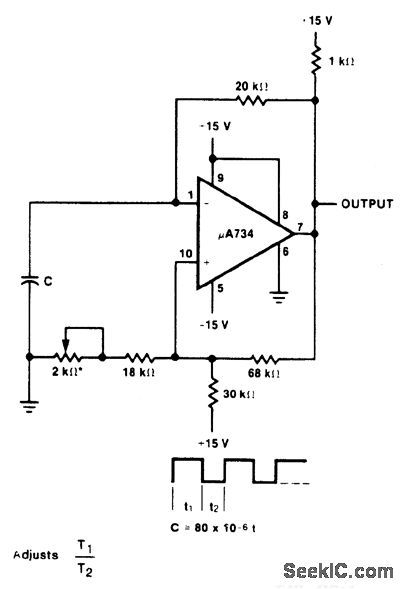
SINGLE_OP_AMP_OSCILLATOR
Published:2009/6/25 4:40:00 Author:May
This circuit has a Schmitt trigger and in-tegrator built around one op amp. Timing is controlled by the RC network. Voltage at the inverting input follows the RC charging expo-nential within the upper and lower hysteresis levels. By closing the switch SWt, the dis-charge time of the capacitor becomes ten times as fast as the rise time. Thus a square wave with an 10:1 mark space ratio is generated. (View)
View full Circuit Diagram | Comments | Reading(1353)
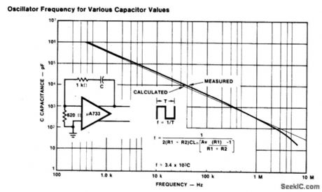
PIERCE_HARMONIC_OSCILLATOR(100_MHz)
Published:2009/6/25 3:10:00 Author:May
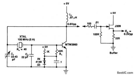
Circuit Notes
The output resistance of the transistor's collector, together with the effective value of C1, provides an RC phase lag of 30-500. The crystal normally oscillates slightly above series resonance, where it is both resistive and inductive. Above series resonance, the crys-tal's internal impedance (resistive and induc-tive) together with C2 provides an RLC phase lag of 130-1500. The transistor inverts the sig-nal, providing a total of 3600 of phase shift around the loop. Inductor L1 is selected to resonate with C1 at a frequency between the crystal's desired harmonic and its next lower odd harmonic. Inductor L1 offsets part of the negative reactance of C1 at the oscillation fre-quency. (View)
View full Circuit Diagram | Comments | Reading(1424)
CMOS_OSCILLATOR_1_MHz_4_MHz
Published:2009/6/25 3:07:00 Author:May
View full Circuit Diagram | Comments | Reading(773)
JFET_PIERCE_CRYSTAL_OSCILLATOR__
Published:2009/6/25 3:04:00 Author:May
Circuit Notes TheJFET Pierce crystal oscillator allowsa wide frequency range of crystals to be usedwithout circuit modification,Since the JFETgate does not load the crystal, good Q IS maln-tained,thus lnsurlng good frequency stability. (View)
View full Circuit Diagram | Comments | Reading(1156)
| Pages:41/54 At 204142434445464748495051525354 |
Circuit Categories
power supply circuit
Amplifier Circuit
Basic Circuit
LED and Light Circuit
Sensor Circuit
Signal Processing
Electrical Equipment Circuit
Control Circuit
Remote Control Circuit
A/D-D/A Converter Circuit
Audio Circuit
Measuring and Test Circuit
Communication Circuit
Computer-Related Circuit
555 Circuit
Automotive Circuit
Repairing Circuit