
D/A Converter
Index
AD7543 12 - bit D / A converter
Published:2013/1/25 1:01:00 Author:Ecco | Keyword: 12 - bit D / A converter
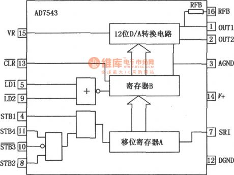
AD7543 has serial input and slower number passing, but the desired signal wiring is less, and it is convenient for optocoupler isolation, it is suitable for telecommunication applications, therefore, it is easily connected with the microcontroller. Similar model: MP7543, and its reference voltage is supplied by an external voltage. AD7543's pinout and internal block diagram is shown as figure:
(View)
View full Circuit Diagram | Comments | Reading(1103)
HDAC7542 12 - bit parallel port D / A converter
Published:2013/1/22 2:48:00 Author:Ecco | Keyword: 12 - bit, parallel port, D / A converter

HDAC7542 can be directly matched with CPU, and it is a low-power, high-speed, high - gain 12-bit multiplying D / A converter. The digital signal is divided into 3 groups which is input tp memory by 4 bytes, and its internal data is written to the D / A converter after passing cache twice, then the D / A converter output is updated for four-quadrant multiplication. Its typical application circuit is shown as figure. Figure (A) shows the unipolar 2-quadrant multiplying connection.
(View)
View full Circuit Diagram | Comments | Reading(1259)
ISOLATED_3_V_TO_5_V_DAC
Published:2009/7/12 22:50:00 Author:May
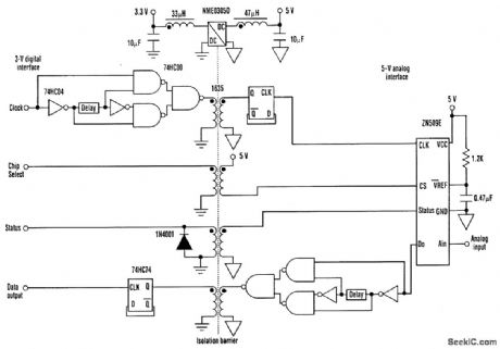


The circuit uses a low-power (1 W) dc-to-dc converter for the power isolation and a transformer isolator/translator for the data interface. The transformer isolator not only provides the galvanic iso-lation required, but also converts the data signals between 3-V and 5-V levels. As a result, no additional level conversion is required. The ADC can run at 1-MHz clock rates. To allow the 50 percent duty cycles (clock and data signals) to pass through a transformer isolator requires an edge-detection and conversion technique. The edge detector is built from simple logic gates (two inverters and three NAND gates) and a short delay (either a delay line or a passive RC circuit can be used). The signal is rebuilt with a D-type flip-flop. Using a four-channel isolator allows full control over the ADC to be exercised. Conversion is requested by pulling the Chip Select pin low, and a Status high for one clock cycle is reported back to acknowledge conversion start. The first data bit (MSB) then is presented onto the data line, and all eight bits are transferred with a further Status signal at the end of conversion. Conversion can be requested asynchronously with the system clock, if necessary, and the Status flag can be used to poll the controlling logic circuitry. Filtering is placed on either side of the dc-to-dc converter to reduce power-supply ripple and prevent noise on the logic power supply from affecting the analog system. Although not shown, all ICs have 0.22-μF decoupling capacitors. (View)
View full Circuit Diagram | Comments | Reading(1160)
FOUR_QUADRANT_MULTIPLYING_DAC
Published:2009/7/7 22:41:00 Author:May
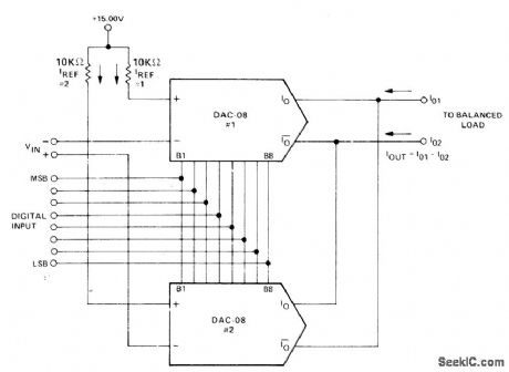
Combination of two Precision Monolithics DAC-08 D/A conveners accepts differential input voltage and produces differential current output, 0ut-put opamp is not normally required. Output analog polarity is controlled by analog input ref-erence or by offset-binary digital input word. Common-mode current present at output must be accommodated by balanced load. Differential input range is 10 V.-J. Schoeff and D. Soderquist, Differential and Multiplying Digital to Analog Converter Applications, Precision Monolithics, Santa Clara, CA, 1976, AN-19, p 3. (View)
View full Circuit Diagram | Comments | Reading(1264)
DIGITAL_TO_FREQUENCY
Published:2009/7/7 4:26:00 Author:May
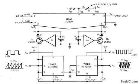
Combination of multiplying DAC and 556 dual timer provides complementary output frequencies under con trol of digital input. Opamp and diode types are not critical. Output frequency of each timer depends on supply voltages, capacitor values,and setting of R1.-J. Wilson and J. Whitmore,MDAC's Open Up a New World of Digital-Control Applications,EDN Magazine,Sept.20、1978、p 97-105. (View)
View full Circuit Diagram | Comments | Reading(916)
1500_V_ISOLATION_FOR_DAC
Published:2009/7/6 7:51:00 Author:May
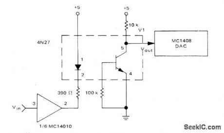
Motorola 4N27 optoisolator provides required isolation between DAC of programmable power supply and remotely located CMOS MC14010 noninverting buffer.-D. Aldridge and N. Wellenstein, Designing Digitally-Controlled Power Supplies, Motorola, Phoenix, AZ, 1975, AN-703, p 9. (View)
View full Circuit Diagram | Comments | Reading(1356)
FOUR_OUADRANT_ALGEBRAIC
Published:2009/6/30 3:21:00 Author:May

Two Precision Monolithics DAC-08 D/A converters perform fast algebraic summation of two digital input words and feed OP-02 opamp that provides direct analog output which is algebraic sum of words A and B in all four quadrants.—J. Schoeff and D. Soderquist, Differential and Multiplying Digital to Analog Converter Applications, Precision Monolithics, Santa Clara, CA, 1976, AN-19, p 7. (View)
View full Circuit Diagram | Comments | Reading(1592)
SIMPLE_DAC
Published:2009/6/30 3:05:00 Author:May
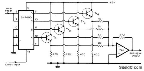
Transistors are either saturated or cut off by outputs of clock-controlled SN7490 BCD counter, Portions of emitter voltages of the four transistors are added in ratios 1:2:4:8 by 741 summing opamp to obtain analog output. Article tells how two such circuits can be combined for use in two-digit DVM.—D. James, Simple Digital to Analogue Converter, Wireless World, June 1974, p 197. (View)
View full Circuit Diagram | Comments | Reading(2400)
ANALOG_SUM_OF_DIGITAL_NUMBERS
Published:2009/6/30 3:04:00 Author:May
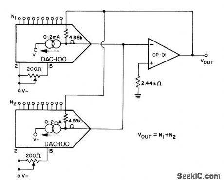
Two Precision Monolithics DAC-100 D/A convelters and op-01 opamp combine conversion with adding to give high-precision DC output voltage,200-ohm pots are adjusted initially to give exactly desired output for input of all 0s,— 8 &10 Bit Digital-to-Analog Converter, Precision Monolithics, Santa Clara, CA, 1977、DAC-100, p 5. (View)
View full Circuit Diagram | Comments | Reading(976)
DAC_FOR_SPEECH
Published:2009/6/30 3:00:00 Author:May
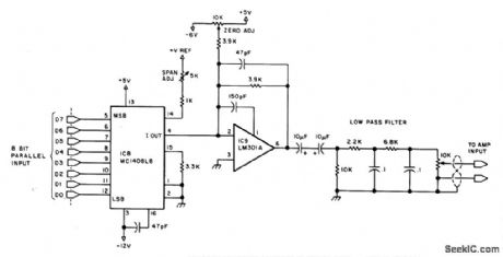
Audio signals stored in 8-channel digital form in computer are converted back into analog form for feed through low-pass filter to input of audio amplifier. Can be used for computer-controlled synthesis of speech from phonemes in any language or for providing voice replies to queries. Pin 7 of IC9 is +12 V, and pin 4 is -12V.—S. Ciarcia, Talk to Me! Add a Voice to Your Computer for $35, BYTE, June 1978, p 142-151 (View)
View full Circuit Diagram | Comments | Reading(1622)
HIGH_SPEED_VOLTAGE_OUTPUT_DAC
Published:2009/6/26 2:57:00 Author:May
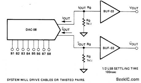
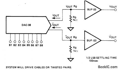
View full Circuit Diagram | Comments | Reading(0)
±10_V_FULL_SCALE_UNIPOLAR_DAC
Published:2009/6/26 2:51:00 Author:May
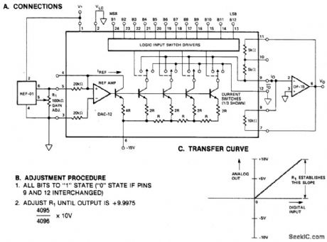
View full Circuit Diagram | Comments | Reading(0)
16_BIT_BINARY_DAC
Published:2009/6/26 2:43:00 Author:May
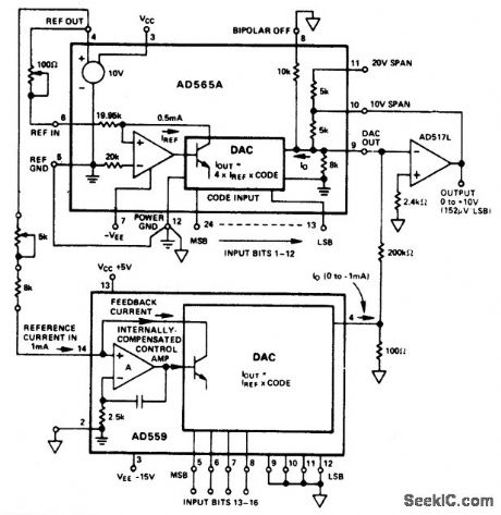
View full Circuit Diagram | Comments | Reading(0)
8_BIT_D_A_WITH_OUTPUT_CURRENT_TO_VOLTAGE_CONVERSION
Published:2009/6/26 2:40:00 Author:May
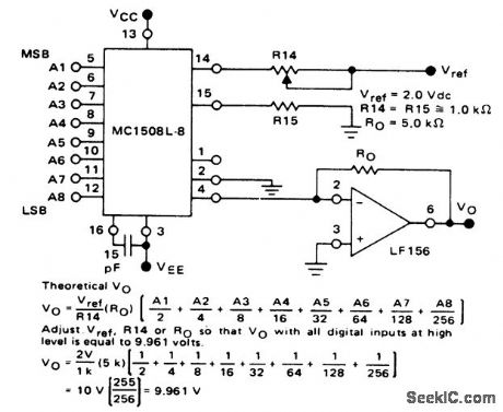
View full Circuit Diagram | Comments | Reading(0)
±10_V_FULL_SCALE_BIPOLAR_DAC
Published:2009/6/26 2:37:00 Author:May
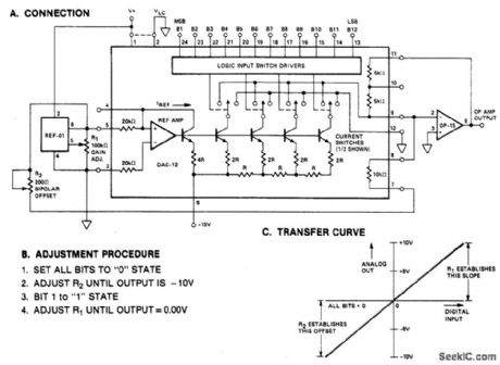
View full Circuit Diagram | Comments | Reading(0)
PRECISION_12_BIT_D_A_CONVERTER
Published:2009/6/26 2:35:00 Author:May

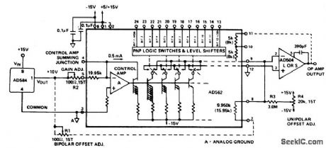
View full Circuit Diagram | Comments | Reading(0)
10_BIT,4_QUADRANT_MULTIPLEXING_D_A_CONVERTER(OFFSET_BINARY_CODING)
Published:2009/6/26 2:29:00 Author:May
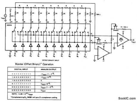
View full Circuit Diagram | Comments | Reading(969)
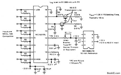
HIGH_SPEED_8_BIT_D_A_CONVERTER
Published:2009/6/26 2:23:00 Author:May
View full Circuit Diagram | Comments | Reading(977)
8_BIT_D_A_CONVERTER
Published:2009/6/26 2:21:00 Author:May

View full Circuit Diagram | Comments | Reading(1330)
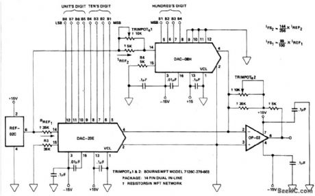
THREE_DIGIT_BCD_D_A_CONVERTER
Published:2009/6/26 2:17:00 Author:May
View full Circuit Diagram | Comments | Reading(899)
| Pages:1/2 12 |
Circuit Categories
power supply circuit
Amplifier Circuit
Basic Circuit
LED and Light Circuit
Sensor Circuit
Signal Processing
Electrical Equipment Circuit
Control Circuit
Remote Control Circuit
A/D-D/A Converter Circuit
Audio Circuit
Measuring and Test Circuit
Communication Circuit
Computer-Related Circuit
555 Circuit
Automotive Circuit
Repairing Circuit